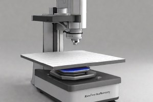
Electron Beam Induced Current (EBIC) Testing for Semiconductor Defects
Electron Beam Induced Current (EBIC) is a semiconductor analysis technique utilizing SEM or STEM to create electron-hole pairs and measuring the variable induced currents (EBIC) at p-n or Schottky junctions, or defect locations. Infinita Lab offers this test to clients in the USA and across the world, utilizing its large laboratory network.

TRUSTED BY


Precision-driven testing for dimensional accuracy and compliance
- Overview
- Scope, Applications, and Benefits
- Test Process
- Specifications
- Instrumentation
- Results and Deliverables
Overview
Electron Beam Induced Current is an advanced characterization technique used to study electrical activity and defects in semiconductor materials. It works by scanning a focused electron beam over a sample and measuring the induced current generated within the material.
This technique is widely used in the semiconductor, electronics, and materials science industry to analyze junction properties, carrier recombination, and defect distribution in devices such as diodes, transistors, and solar cells. EBIC provides high-resolution insight into electrical behavior at the micro and nanoscale, making it essential for failure analysis and device optimization.

Scope, Applications, and Benefits
Scope
EBIC analysis evaluates electrical response and defect activity in semiconductor materials using electron beam interaction.
It helps identify recombination sites, junction behavior, and material inconsistencies.
- Semiconductor defect characterization
- Junction property evaluation
- Carrier recombination analysis
- Electrical activity mapping
- Failure analysis
- Device performance assessment
- Quality control and validation
Applications
- Semiconductor device analysis
- Solar cell characterization
- Integrated circuit inspection
- Failure analysis of electronic components
- Research and material development
Benefits
- High-resolution electrical mapping
- Detects micro and nano-scale defects
- Improves device performance
- Supports failure analysis
- Enhances material quality
- Enables precise diagnostics
- Aids advanced research
Test Process
Sample Preparation
Semiconductor sample is prepared with electrical contacts for current collection.
1Electron Beam Scanning
Focused electron beam scans the sample surface in a controlled pattern.
2Current Generation
Electron interaction generates charge carriers collected as induced current.
3Mapping and Analysis
Current signals are mapped to identify defects and junction behavior.
4Technical Specifications
| Parameter | Details |
|---|---|
| Material Type | Semiconductor materials and devices. |
| Measured Parameter | Induced current signal. |
| Resolution | Micro to nanoscale spatial resolution. |
| Operating Environment | Vacuum conditions in SEM chamber. |
| Signal Detection | Sensitive current amplifiers. |
| Temperature Condition | Ambient or controlled temperature. |
Instrumentation Used for Testing
- Scanning Electron Microscope (SEM)
- EBIC detector system
- Current amplifier
- Sample stage with electrical contacts
- Data acquisition system
- Vacuum chamber
Results and Deliverables
- EBIC current maps
- Defect location identification
- Junction behavior analysis
- Carrier recombination data
- Device performance insights
- Test documentation
- Final technical report
Why Choose Infinita Lab for EBIC?
With Infinita Lab (www.infinitalab.com), you are guaranteed a Nationwide Network of Accredited Laboratories spread across the USA, the best Consultants from around the world, Convenient Sample Pick-Up and Delivery, and Fast Turnaround Time.
Our team understands the stakes and subtleties of every test. Whether you’re validating a new Product, de-risking a prototype, or navigating complex compliance requirements, our specialists guide the process with rigor and clarity.
Looking for a trusted partner to achieve your research goals? Schedule a meeting with us, send us a request, or call us at (888) 878-3090 to learn more about our services and how we can support you. Request a Quote
Frequently Asked Questions
EBIC is a technique that uses an electron beam to generate and measure current in semiconductor materials, helping analyze electrical activity, defects, and junction properties in electronic devices and materials at very high spatial resolution.
A focused electron beam scans the sample, generating electron-hole pairs that produce a measurable current. Variations in this current reveal defects, recombination sites, and electrical behavior across the material.
It helps identify electrically active defects that may not be visible through standard imaging, enabling accurate root cause analysis of device failures.
EBIC provides both spatial imaging and electrical information simultaneously, offering deeper insights into material behavior compared to purely structural imaging methods.
Factors include beam energy, sample preparation, electrical contact quality, and material properties, all of which influence signal strength and accuracy.

Request a Quote
Submit your material details and receive testing procedures, pricing, and turnaround time within 24 hours.
 Quick Turnaround and Hasslefree process

 Confidentiality Guarantee

 Free, No-obligation Consultation

 100% Customer Satisfaction


