Reality Time X-Ray Inspection and Imaging Analysis
X-Ray Inspection and Imaging Analysis in real time
X-ray inspection and imaging analysis in real-time are done by Soldering the Interconnection Bump Wire Bond Breakage Solder Void Short / Open Circuits Missing Solder Balls, Drill quality, Die to attach, and Solder Joint Void Offset.
A sample can be internally inspected while being moved and rotated using real-time X-ray technology. If there are any internal flaws or concealed problems, they can be found by looking at the sample’s internal construction. The microelectronic, semiconductor, aerospace, and automotive industries can internally inspect small devices, packages, and components with high magnification and resolution thanks to ITL’s X-Ray Systems.
This non-destructive method provides a quick and in-depth investigation of structures with different densities. Printed circuit boards, ceramic, metal, and plastic packages, ball grid arrays, and other electrical and automotive components are among the applications.
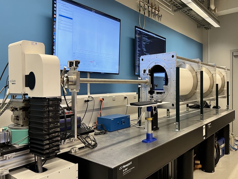
The Nicolet NXR-1400 X-ray Inspection System features a side window x-ray tube, a 120 kV x-ray source with a 10 m focused spot, and 65x magnification capability.
The 10 to 110 kV x-ray source is used in the Hewlett-Packard Faxitron 43855 A cabinet x-ray system.
 Metrology Testing Service

- Tensiometry
- Rutherford Backscattering Spectrometry (RBS): Advanced Thin Film and Surface Analysis
- FTIR Services In The Electronics Failure Analysis Lab
- Nuclear Magnetic Resonance Spectroscopy (NMR)
- Specular X-ray Reflectivity (XRR)
- Electrical Calibration
- Dynamic Mechanical Analysis (DMA)
- Flow Calibration
- View All


3 Easy Steps to Start Testing


Case Studies
In-depth examination of genuine material testing solutions
Dopant and Ultra-Low Concentration Elemental Analysis Using STEM…

Dopant and Ultra-Low Concentration Elemental Analysis Using STEM…
Introduction to STEM-EELS for Elemental Analysis Scanning Transmission Electron Microscopy (STEM) combined with Electron Energy Loss...
Read Case StudyAnalysis of PVC Pipe Degradation Using FTIR Spectroscopy

Analysis of PVC Pipe Degradation Using FTIR Spectroscopy
PVC Pipe in Infrastructure — and Why Degradation Matters Polyvinyl chloride (PVC) pressure pipe is one...
Read Case StudyNano-scale roughness measurement of Si-wafers by Atomic Force…

Nano-scale roughness measurement of Si-wafers by Atomic Force…
Nano-scale surface roughness is a critical parameter in fabricated thin-films that are used in optics, solar...
Read Case StudyTalk to Our Experts Today!
Submit your contact info and we’ll get back to you within 24 hours
