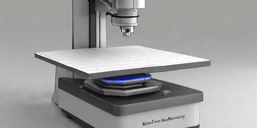
Atomic Force Microscopy (AFM) Testing & Surface Characterization
Atomic Force Microscopy (AFM) is a non-optical surface topographic analysis technique with high lateral (nm), vertical (Aº), and force (pN) resolution. AFM is used to obtain high-resolution nanoscale images and study local sites of micro/nanostructured coatings and surfaces.
TRUSTED BY


Precision-driven testing for dimensional accuracy and compliance
- Overview
- Scope, Applications, and Benefits
- Test Process
- Specifications
- Instrumentation
- Results and Deliverables
Overview
Atomic Force Microscopy (AFM) is an accurate method to observe the way something looks on the nanometer scale in terms of its form, texture, and other tiny features. It does this by scanning the surface of the object with a pointed probe attached to a spring-like structure called a cantilever. The interaction between the probe and the object causes the cantilever to change its position, which is then detected by a laser to produce an image.
The result is an image of the object in three dimensions, with nanometer or even atomic resolution. AFM is used in fields like nanotechnology, materials science, semiconductor research, polymers, and biology, where surface properties and microstructures are important.

Scope, Applications, and Benefits
Scope
Atomic Force Microscopy (AFM) is an advanced surface analysis technique that allows for the observation of surface features at the nanoscale for various materials. The technique involves sliding a sharp tip on the surface of the material and is capable of producing rich 3D images that show the interaction of the surface at nanometre distances. The technique has gained prominence in various fields, including materials science, nanotechnology, semiconductor studies, and biology.
AFM is capable of analysing:
– Polymers
– Thin films and coatings
– Semiconductor materials
– Nanomaterials and nanoparticles
– Metals and alloys
– Ceramics and composites
Applications
- Surface morphology analysis
- Nanostructure characterization
- Thin film thickness evaluation
- Polymer surface studies
- Semiconductor wafer inspection
- Nanotechnology research
- Coating and surface engineering analysis
- Failure analysis and defect detection
Benefits
- Extremely high spatial resolution
- Three-dimensional surface imaging
- Minimal sample preparation required
- Non-destructive analysis capability
- Applicable to conductive and non-conductive materials
- Quantitative measurement of nanoscale features
- Multiple imaging modes for different properties
Test Process
Sample Preparation
The sample is cleaned and mounted on the AFM stage.
1Probe Interaction
A sharp probe interacts with the surface at the nanoscale.
2Surface Scanning
The probe scans the surface in a raster pattern to detect features.
3Detection & Imaging
Cantilever deflections are measured to generate a 3D surface image.
4Technical Specifications
| Parameter | Details |
|---|---|
| Resolution | Nanometre to atomic-level resolution |
| Imaging Modes | Contact mode, tapping mode, non-contact mode |
| Measured Parameters | Surface roughness, height profile, grain size, adhesion, friction |
| Applicable Materials | Polymers, metals, ceramics, semiconductors, nanomaterials |
| Output Format | 3D surface topography maps and quantitative surface parameters |
Instrumentation Used for Testing
- Atomic force microscope system
- Cantilever probes with nanoscale tips
- Laser detection system
- Photodiode detector
- Piezoelectric scanner
- Vibration isolation stage
- Computer with AFM control and analysis software
Results and Deliverables
- High-resolution 3D surface images
- Surface roughness measurements
- Grain size and nanoscale feature analysis
- Topography and height profile maps
- Adhesion and friction measurements
- Comparative surface analysis reports
Partnering with Infinita Lab for Optimal Results
Infinita Lab addresses the most frustrating pain points in the Atomic Force Microscopy – AFM testing process: complexity, coordination, and confidentiality. Our platform is built for secure, simplified support, allowing engineering and R&D teams to focus on what matters most: innovation. From kickoff to final report, we orchestrate every detail—fast, seamlessly, and behind the scenes.
Looking for a trusted partner to achieve your research goals? Schedule a meeting with us, send us a request, or call us at (888) 878-3090 to learn more about our services and how we can support you. Request a Quote
Frequently Asked Questions
AFM can analyze a wide variety of materials including polymers, metals, ceramics, semiconductors, thin films, coatings, nanomaterials, and biological samples such as cells and proteins.
AFM provides detailed information about surface topography, roughness, grain size, nanoscale features, and mechanical properties such as adhesion and friction at the nanoscale.
The most common AFM imaging modes include contact mode, tapping mode (intermittent contact), and non-contact mode. Each mode is suitable for different types of samples and surface characteristics.
No. AFM typically requires minimal sample preparation. The sample surface only needs to be clean and securely mounted on the instrument stage.
AFM offers extremely high spatial resolution, typically in the nanometre range and sometimes even at atomic-level resolution depending on the sample and instrument configuration.


Request a Quote
Submit your material details and receive testing procedures, pricing, and turnaround time within 24 hours.
 Quick Turnaround and Hasslefree process
 Confidentiality Guarantee
 Free, No-obligation Consultation
 100% Customer Satisfaction
