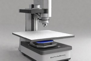
Differential Hall Effect Metrology (DHEM)
Differential Hall Effect Metrology (DHEM) measures critical electrical properties at depths upto a few nanometers in semiconductor samples. Successive layers of the sample are exposed by etching or oxidation and sheet resistance and mobility measurements performed using Hall effect and Van der Pauw techniques. Infinita Lab, USA, offers this test to clients in the USA and across the world, through its laboratory network.

TRUSTED BY


Precision-driven testing for dimensional accuracy and compliance
- Overview
- Scope, Applications, and Benefits
- Test Process
- Specifications
- Instrumentation
- Results and Deliverables
Overview
Differential Hall Effect Metrology (DHEM) is an advanced technique used to characterize electrical properties such as carrier concentration, mobility, and resistivity in semiconductor materials using differential Hall measurements.
This method is widely applied in the semiconductor and electronics industry for precise analysis of thin films, multilayer structures, and complex device architectures where conventional Hall measurements have limitations.

Scope, Applications, and Benefits
Scope
DHEM enables detailed electrical characterization of semiconductor materials by separating layer-specific properties and improving measurement accuracy.
It supports advanced material analysis, process optimization, and quality control in semiconductor device fabrication.
- Carrier concentration profiling
- Mobility and resistivity measurement
- Thin film and multilayer analysis
- Semiconductor wafer characterization
- Doping profile evaluation
- Electrical property mapping
- Process optimization support
Applications
- Semiconductor wafers and thin films
- Integrated circuits and microelectronics
- Photovoltaic materials
- Advanced electronic devices
- Research and development labs
Benefits
- High accuracy electrical characterization
- Layer-specific property analysis
- Non-destructive testing method
- Suitable for complex structures
- Enhances device performance evaluation
- Supports process development
- Improves material quality control
Test Process
Sample Preparation
Sample is prepared with proper geometry and electrical contacts for accurate Hall measurements.
1Measurement Setup
Magnetic field and current are applied to generate Hall voltage across the sample.
2Differential Measurement
Multiple measurements are taken under varying conditions to isolate layer-specific properties.
3Data Analysis
Electrical parameters like carrier concentration and mobility are calculated from measured data.
4Technical Specifications
| Parameter | Details |
|---|---|
| Material Type | Semiconductor wafers, thin films, and multilayer structures. |
| Measurement Mode | Differential Hall voltage measurement under varying magnetic fields. |
| Magnetic Field Range | Typically low to moderate fields depending on system design. |
| Temperature Control | Measurements performed at controlled or variable temperatures. |
| Sample Geometry | Defined shapes such as van der Pauw or Hall bar structures. |
| Measured Parameters | Carrier concentration, mobility, resistivity. |
Instrumentation Used for Testing
- Hall Effect Measurement System
- Electromagnet or permanent magnet setup
- Current source and voltmeter
- Probe station
- Temperature control unit
- Data acquisition system
Results and Deliverables
- Carrier concentration data
- Mobility and resistivity values
- Layer-specific electrical properties
- Measurement graphs and analysis
- Semiconductor characterization reports
- Calibration and validation records
- Final test report
Why Choose Infinita Lab for Differential Hall Effect Metrology?
With Infinita Lab (www.infinitalab.com), you are guaranteed a Nationwide Network of Accredited Laboratories spread across the USA, the best Consultants from around the world, Convenient Sample Pick-Up and Delivery, and Fast Turnaround Time.
Our team understands the stakes and subtleties of every test. Whether you’re validating a new Product, de-risking a prototype, or navigating complex compliance requirements, our specialists guide the process with rigor and clarity.
Looking for a trusted partner to achieve your research goals? Schedule a meeting with us, send us a request, or call us at (888) 878-3090 to learn more about our services and how we can support you. Request a Quote
Frequently Asked Questions
DHEM is a technique used to measure electrical properties of semiconductor materials using differential Hall effect measurements, enabling accurate characterization of carrier concentration, mobility, and resistivity in complex structures.
DHEM uses differential measurements to separate contributions from multiple layers, providing more detailed and accurate analysis compared to conventional Hall effect methods.
DHEM helps in precise material characterization, improving device performance, process optimization, and quality control in semiconductor fabrication.
A magnetic field is applied to generate Hall voltage, which is used to calculate electrical properties of the material.
Yes, DHEM is specifically useful for analyzing multilayer semiconductor structures by separating layer-specific electrical properties.
Case Studies
In-depth examination of genuine material testing solutions
Dopant and Ultra-Low Concentration Elemental Analysis Using STEM…
Introduction to STEM-EELS for Elemental Analysis Scanning Transmission Electron Microscopy (STEM) combined with Electron Energy Loss...
Read Case StudyAnalysis of PVC Pipe Degradation Using FTIR Spectroscopy
PVC Pipe in Infrastructure — and Why Degradation Matters Polyvinyl chloride (PVC) pressure pipe is one...
Read Case StudyNano-scale roughness measurement of Si-wafers by Atomic Force…
Nano-scale surface roughness is a critical parameter in fabricated thin-films that are used in optics, solar...
Read Case Study
Request a Quote
Submit your material details and receive testing procedures, pricing, and turnaround time within 24 hours.
 Quick Turnaround and Hasslefree process

 Confidentiality Guarantee

 Free, No-obligation Consultation

 100% Customer Satisfaction


