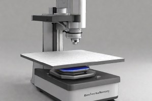
Electron Backscatter Diffraction (EBSD)
Electron Backscatter Diffraction (EBSD) is a microstructural analysis technique for crystalline materials. EBSD uses the diffraction patterns of an incident electron beam, from a scanning electron microscope (SEM), to obtain crystallographic information. The laboratory network of Infinita Lab, USA, offers this test to clients in the USA and other places.

TRUSTED BY


Precision-driven testing for dimensional accuracy and compliance
- Overview
- Scope, Applications, and Benefits
- Test Process
- Specifications
- Instrumentation
- Results and Deliverables
Overview
Electron Backscatter Diffraction (EBSD) is a highly advanced materials analysis technique used to study a wide range of materials, including metals, ceramics, and semiconductors. EBSD analysis is performed using scanning electron microscopy and is used to analyze materials at the microscale. EBSD analysis provides valuable insights into materials and is used for various purposes, such as materials development, quality assurance, and failure analysis.

Scope, Applications, and Benefits
Scope
EBSD is used to analyze crystallographic microstructures by collecting and analyzing electron backscatter diffraction patterns formed when electrons are diffracted from the polished surface of a specimen in a scanning electron microscope.
EBSD analysis evaluates:
- Grain orientation mapping and crystallographic texture analysis of polycrystalline materials
- Grain boundary character distribution, including low and high-angle boundary identification
- Phase identification and discrimination across multi-phase metallic and ceramic material systems
- Residual strain and deformation mapping within material microstructures
- Recrystallization fraction, grain size distribution, and microstructural homogeneity assessment
Applications
- Metals and alloys, including steel, aluminum, titanium, nickel superalloys, and copper systems
- Ceramic, semiconductor, and thin film materials requiring crystallographic characterization
- Welded, deformed, and heat-treated material microstructural assessment
- Failure analysis investigations requiring grain boundary and crystallographic root cause evaluation
- Academic and industrial research programs requiring advanced microstructural characterization data
Benefits
- Provides high-resolution crystallographic and microstructural data unavailable through conventional microscopy
- Supports material development, process optimization
- Identifies crystallographic failure mechanisms in support of root cause failure analysis
- Delivers traceable, quantitative microstructural data
- Reduces material development risk by providing detailed microstructural intelligence early in the design cycle
Test Process
Sample Preparation
Specimens sectioned, mounted, and polished to high-quality surface finish for EBSD pattern acquisition.
1SEM & EBSD Setup
Specimen loaded into SEM, tilted to acquisition angle, and detector configured for optimal pattern quality.
2Data Acquisition
Electron beam rastered across analysis area collecting and indexing diffraction patterns at each point.
3Data Analysis & Reporting
EBSD datasets processed to generate orientation maps, pole figures, and microstructural statistics.
4Technical Specifications
| Parameter | Details |
|---|---|
| Applicable Materials | Metals, alloys, ceramics, semiconductors, thin films, and polycrystalline materials |
| Analysis Technique | Electron backscatter diffraction pattern collection and indexing within SEM |
| Spatial Resolution | Sub-micron crystallographic orientation mapping capability |
| Measured Parameters | Grain orientation, texture, phase distribution, grain boundary character, residual strain |
| Measured Outputs | Orientation maps, pole figures, grain boundary maps, phase maps, microstructural statistics |
Instrumentation Used for Testing
- Field emission scanning electron microscope with EBSD detector system
- Automated pattern acquisition and indexing software
- Specimen preparation equipment, including grinding, polishing, and electropolishing systems
- Colloidal silica and OPS final polishing consumables
- Specialist EBSD analysis and post-processing software
- Data reporting and visualization system
Results and Deliverables
- EBSD orientation and phase maps with defined analysis area and step size documentation
- Pole figures and inverse pole figures for crystallographic texture characterization
- Grain boundary character distribution maps and quantitative boundary statistics
- Grain size distribution, recrystallization fraction, and microstructural homogeneity data
- Comprehensive EBSD analysis report
Why Choose Infinita Lab for Electron Backscatter Diffraction (EBSD)?
Infinita Lab is a trusted USA-based testing laboratory offering Electron Backscatter Diffraction (EBSD) testing services across an extensive network of accredited facilities across the USA. Infinita Lab is built to serve the full spectrum of modern testing needs—across industries, materials, and methodologies. Our advanced equipment and expert professionals deliver highly accurate and prompt test results, helping businesses achieve quality compliance and product reliability.
Looking for a trusted partner to achieve your research goals? Schedule a meeting with us, send us a request, or call us at (888) 878-3090 to learn more about our services and how we can support you. Request a Quote
Frequently Asked Questions
EBSD is a technique that utilizes SEM for materials characterization. In EBSD, the electron beam is scanned across a tilted crystalline sample, and diffracted electrons at each point form a pattern, which can be detected and then analyzed using dedicated hardware and software.
Electron Backscatter Diffraction (EBSD) has a resolution ranging from 50 nm to several microns, depending upon sample quality and setup. A spatial resolution of about 1 micron should be possible for routine applications.
EBSD is significant in material science as the information obtained from this technique includes degree of orientation, phase identification, grain boundary characterization, and defect analysis, which are essential for understanding material properties.
EBSD analyzes various crystalline materials, including metals, ceramics, rocks, semiconductors, and ice, to gain insights into their microstructure and crystallography.
EBSD requires sample preparation, as mechanical grinding or polishing can distort the surface crystal lattices. Moreover, insulators may demand conductive coatings, affecting their precision analysis.
Case Studies
In-depth examination of genuine material testing solutions
Dopant and Ultra-Low Concentration Elemental Analysis Using STEM…
Introduction to STEM-EELS for Elemental Analysis Scanning Transmission Electron Microscopy (STEM) combined with Electron Energy Loss...
Read Case StudyAnalysis of PVC Pipe Degradation Using FTIR Spectroscopy
PVC Pipe in Infrastructure — and Why Degradation Matters Polyvinyl chloride (PVC) pressure pipe is one...
Read Case StudyNano-scale roughness measurement of Si-wafers by Atomic Force…
Nano-scale surface roughness is a critical parameter in fabricated thin-films that are used in optics, solar...
Read Case Study
Request a Quote
Submit your material details and receive testing procedures, pricing, and turnaround time within 24 hours.
 Quick Turnaround and Hasslefree process

 Confidentiality Guarantee

 Free, No-obligation Consultation

 100% Customer Satisfaction


