Scanning Acoustic Tomography (SAT)
Scanning Acoustic Tomography is a non-destructive technique that analyses the structural composition of a material. It is used to detect hidden defects and voids in materials. It provides three-dimensional images.

TRUSTED BY


Precision-driven testing for dimensional accuracy and compliance
- Overview
- Scope, Applications, and Benefits
- Test Process
- Specifications
- Instrumentation
- Results and Deliverables
Overview
Scanning Acoustic Tomography (SAT) is a non-destructive testing technique that uses high-frequency ultrasonic waves to detect any internal defects in a material or electronic component. SAT is a non-destructive technique that creates acoustic images of a component and provides information about its internal structures without any damage to the component.
SAT is a non-destructive technique that is commonly applied to inspect semiconductor packages, electronic components, composite structures, and bonded structures. SAT is useful in detecting defects in a component, such as delamination, voids, cracks, and bonding.

Scope, Applications, and Benefits
Scope
Scanning Acoustic Tomography evaluates the internal integrity of materials and electronic components using ultrasonic imaging techniques. The method enables detection of hidden defects and structural irregularities without altering or damaging the test specimen.
The scope includes:
Detection of internal defects and delamination
Inspection of semiconductor and electronic packages
Evaluation of bonding and interface integrity
Identification of voids, cracks, and inclusions
Non-destructive evaluation of composite materials
Applications
Semiconductor and microelectronic components
Printed circuit boards (PCBs)
Integrated circuit (IC) packages
Composite materials and bonded structures
Electronics manufacturing and quality control
Benefits
Non-destructive inspection method
Detects hidden internal defects
Provides high-resolution acoustic images
Improves product reliability and performance
Supports failure analysis and quality assurance
Test Process
Sample Preparation
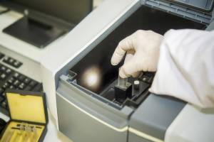
The specimen is cleaned and placed in the testing system, often immersed in a water medium for acoustic transmission.
1Ultrasonic Scanning
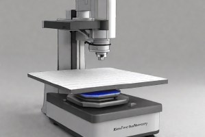
High-frequency ultrasonic waves are transmitted into the specimen using a scanning microscope.
2Signal Detection
Reflected acoustic signals from internal structures are captured by sensors.
3Image Analysis
The collected signals are processed to generate acoustic images that reveal internal defects and structural features.
4Technical Specifications
| Parameter | Details |
|---|---|
| Frequency Range | Typically 10–300 MHz |
| Inspection Type | Non-destructive evaluation (NDT) |
| Imaging Mode | A-scan, B-scan, and C-scan |
| Applicable Materials | Electronics, composites, bonded structures |
| Test Medium | Water or acoustic coupling liquid |
| Output Data | Acoustic images and defect mapping |
Instrumentation Used for Testing
Scanning Acoustic Microscope (SAM)
Ultrasonic Transducer
Water Coupling Tank
Signal Processing Unit
Imaging and Analysis Software
Results and Deliverables
Acoustic scan images (A-scan, B-scan, C-scan)
Identification of internal defects
Delamination and void detection report
Structural integrity evaluation
Detailed inspection report with analysis
Why Choose Infinita Lab for Scanning Acoustic Tomography (SAT)?
Infinita Lab is a leading provider of Scanning Acoustic Tomography (SAT) and streamlined material testing services, addressing the critical challenges faced by emerging businesses and established enterprises. With access to a vast network of over 2,000+ accredited partner labs across the United States, Infinita Lab ensures rapid, accurate, and cost-effective testing solutions. The company’s unique value proposition includes comprehensive project management, confidentiality assurance, and seamless communication through a Single Point of Contact (SPOC) model. By eliminating inefficiencies in traditional material testing workflows, Infinita Lab accelerates research and development (R&D) processes.
Looking for a trusted partner to achieve your research goals? Schedule a meeting with us, send us a request, or call us at (888) 878-3090 to learn more about our services and how we can support you. Request a Quote
Frequently Asked Questions
Scanning Acoustic Tomography (SAT) is a non-destructive ultrasonic imaging technique used to inspect the internal structure of materials and electronic components. It helps detect hidden defects such as delamination, voids, cracks, and bonding issues.
SAT can detect internal defects including delamination between layers, air voids, cracks, inclusions, and poor adhesive bonding. These defects are often invisible externally but can affect the reliability and performance of electronic or composite components.
SAT testing is widely used in semiconductor, electronics manufacturing, aerospace, automotive, and composite industries. It is particularly useful for inspecting microelectronic packages, circuit boards, and layered materials where internal defects must be detected.
SAT systems typically operate with ultrasonic frequencies ranging from approximately 10 MHz to 300 MHz. Higher frequencies provide improved resolution, enabling detailed imaging of small internal features and microscopic defects.
SAT helps detect hidden internal defects during manufacturing and quality inspection. By identifying issues such as delamination or voids early, manufacturers can prevent product failures and improve long-term reliability of electronic devices.
Case Studies
In-depth examination of genuine material testing solutions
Case Study: Dopant & Ultra-Low Concentration Analysis via…
Introduction to STEM-EELS for Elemental Analysis Scanning Transmission Electron Microscopy (STEM) combined with Electron Energy Loss...
Read Case StudyAnalysis of PVC Pipe Degradation Using FTIR Spectroscopy
PVC Pipe in Infrastructure — and Why Degradation Matters Polyvinyl chloride (PVC) pressure pipe is one...
Read Case StudyNano-scale roughness measurement of Si-wafers by Atomic Force…
Nano-scale surface roughness is a critical parameter in fabricated thin-films that are used in optics, solar...
Read Case Study
Request a Quote
Submit your material details and receive testing procedures, pricing, and turnaround time within 24 hours.
 Quick Turnaround and Hasslefree process

 Confidentiality Guarantee

 Free, No-obligation Consultation

 100% Customer Satisfaction


