


Scanning Electron Microscopy (SEM)
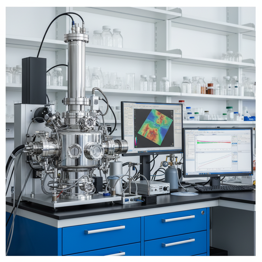
Energy Dispersive X-ray Spectroscopy (EDXS) with scanning electron microscopy (SEM) (EDS).The Scanning Electron Microscope (SEM), which enables the investigation of both the morphology and composition of biological and physical materials, is one of the most adaptable and frequently used scientific instruments today.


Scanning Electron Microscopy testing
Using electron microscopes, it is possible to examine objects at extremely small scales. The following information can be obtained from this examination:
- Topography
The surface characteristics of an object, or “how it looks,” as well as its texture, have a direct relationship to the attributes of the material (hardness, reflectivity, etc.).
- Morphology
The relationship between these structures and the qualities of the material (ductility, strength, reactivity, etc.), as well as the shape and size of the particles that make up the object.
- Composition
The elements and compounds that make up the thing and their proportionate proportions; the connection between composition and a material’s physical characteristics (such as melting point, reactivity, hardness, etc.).
Information about crystals
The arrangement of atoms within an object and how those arrangements directly relate to the qualities of the material (conductivity, electrical properties, strength, etc.).
High-resolution morphology or topography photographs of a specimen can be acquired by scanning an electron probe across it, providing a significant depth of field at either very low or very high magnifications. Monitoring secondary X-rays generated by the interaction between an electron and a sample can also be used to determine a material’s composition. Therefore, multi-phase materials or complex, bio-active materials can be used to create precise maps of elemental distribution. It is possible to characterize fine particulate matter in terms of its size, shape, and distribution as well as to statistically analyze these factors.
Our scanning electron microscope (SEM) is a cutting-edge, ultra-high-resolution microscope with a cutting-edge digital image processing system. It is a highly helpful tool for researching IC wafers, photoresist evaluation, IC research and development, IC production methods, material science, biological research, and industrial research.
Energy Dispersive Spectroscopy (EDS) is a spectrographic method that provides qualitative and semi-quantitative data by identifying the elemental makeup of individual particles in a sample matrix. Combining SEM and EDS procedures results in a strong and adaptable tool that can gather a variety of information.
Common Applications
- Measuring microscopic features
- Checking the product’s integrity
- Review of thin coatings
- Analyzing and identifying the microstructures present on the sample surface
- Failure evaluation
- Assessment of surface contamination
- Polymer identification of inorganic inclusions or pollutants
- Identification of minerals: enables evaluation of the quality of processed ore materials
- The evaluation of corrosion products is made possible by the analysis of metals or oxides.
Video1: The Scanning Electron Microscope
 Metrology Testing Service

- Dual-Beam FIB-SEM Testing for Nanoscale Cross-Section & Analysis
- Transmission Electron Microscopy (TEM) Analysis Services
- AFM Nano-Scale Roughness Measurement Guide for Silicon Wafers
- Case Study: Dopant & Ultra-Low Concentration Analysis via STEM-EELS
- GC-MS (Gas Chromatography-Mass Spectrometry) Testing Services
- What Is a Coating Thickness Gauge? Types, Methods & How to Use One
- Titrimetry (Titration) Testing: Types, Methods & Analytical Applications
- Residual Stress: Types, Origins & Measurement Methods Explained
- View All


3 Easy Steps to Start Testing


Case Studies
In-depth examination of genuine material testing solutions
Case Study: Dopant & Ultra-Low Concentration Analysis via…
Case Study: Dopant & Ultra-Low Concentration Analysis via…
Introduction to STEM-EELS for Elemental Analysis Scanning Transmission Electron Microscopy (STEM) combined with Electron Energy Loss...
Read Case StudyAFM Nano-Scale Roughness Measurement Guide for Silicon Wafers
AFM Nano-Scale Roughness Measurement Guide for Silicon Wafers
Nano-scale surface roughness is a critical parameter in fabricated thin-films that are used in optics, solar...
Read Case StudyTalk to Our Experts Today!
Submit your contact info and we’ll get back to you within 24 hours


