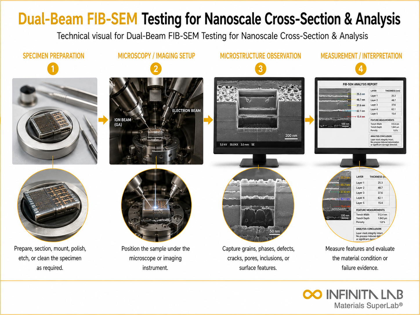


What Is Dual Beam FIB SEM?
Dual Beam – Focused Ion Beam (FIB) is a sophisticated microscopy technique that incorporates a focused ion beam and a scanning electron microscope (SEM) in a single tool. With this tool, precise material removal and cross-sectioning of micro and nanostructures are possible.
Dual beam Focused Ion Beam tools are utilized in various applications, ranging from materials and semiconductor analysis to nanotechnology and failure analysis. The tool is utilized to mill or modify a material’s surface with an ion beam and to provide detailed imaging of structures with an electron beam.

Applications and Benefits of Dual Beam FIB SEM Testing
Scope
Dual Beam FIB analysis enables precise material removal, cross-section preparation, and nanoscale imaging for detailed structural investigation. The technique is particularly useful for examining internal structures and performing site-specific sample preparation.
The scope includes:
Micro and nanoscale material modification
Cross-section preparation of samples
Imaging of internal microstructures
Analysis of semiconductor and electronic devices
Preparation of TEM lamella samples
Applications
Semiconductor device failure analysis
Nanotechnology and microelectronics research
Materials science investigations
Microstructure and interface analysis
TEM sample preparation
Benefits
Enables precise nanoscale milling
Provides high-resolution imaging
Allows site-specific sample preparation
Combines imaging and machining in one system
Supports advanced materials characterization
Our Testing Procedure
Sample Preparation
The specimen is mounted and positioned in the dual beam chamber for analysis.
1Ion Beam Milling
A focused ion beam removes material from the sample to expose internal structures or prepare cross-sections.
2Electron Beam Imaging
The scanning electron beam captures high-resolution images of the exposed surfaces.
3Data Analysis
The images and structural information are analyzed to evaluate material properties or detect defects.
4Test parameters and requirements
| Parameter | Details |
|---|---|
| Technique Type | Dual beam microscopy |
| Ion Source | Gallium ion beam |
| Imaging Method | Scanning electron microscopy |
| Resolution | Nanometer-scale imaging capability |
| Operation Mode | Milling, imaging, and sample preparation |


Dual Beam FIB-SEM System
Focused Ion Beam Source
Scanning Electron Microscope (SEM)
Sample Stage and Chamber
Image Processing Software
Equipment and Instrumentation Used for Testing
What You Receive: Test Report, Data, and Certification
High-resolution microstructure images
Cross-sectional analysis reports
Defect and failure analysis results
Nanoscale structural characterization
Detailed technical analysis repor
Dual Beam FIB SEM FAQs
Dual Beam FIB is an advanced microscopy technique that combines a focused ion beam for precise material removal with a scanning electron microscope for high-resolution imaging and nanoscale structural analysis.
The focused ion beam is used to mill, cut, or remove material from a sample surface, enabling researchers to expose internal structures and prepare precise cross-sections for analysis.
Unlike a conventional SEM, Dual Beam FIB systems include both an ion beam and an electron beam, allowing simultaneous material modification and high-resolution imaging within the same instrument.
Dual Beam FIB enables precise cross-sectioning of microelectronic devices, allowing engineers to examine internal layers, detect defects, and investigate failures in semiconductor components.
Dual Beam FIB systems provide nanoscale resolution imaging and precise material removal, enabling researchers to study microstructures and defects at extremely small dimensions.
Why Choose Infinita Lab for Dual Beam FIB SEM Testing
When your Dual Beam FIB SEM results have to hold up - for compliance, a customer audit, or an engineering decision - accuracy and an unbiased third-party report matter more than price. Infinita Lab routes your dual beam FIB SEM testing to ISO/IEC 17025-accredited U.S. partner labs with hands-on method experience, so you get defensible data, transparent reporting, and turnaround times built around your project deadline - not ours.

Looking for an Accredited Partner for Dual Beam FIB SEM Testing?
Send query us at hello@infinitalab.com or call us at (888) 878-3090 to learn more about our services and how we can support you.