


Microscopic Analysis Testing Services – Optical, SEM & Electron Microscopy
Microscopic analysis is a powerful tool for examining materials in research and industry. It is used to measure foam cell size in rigid cellular plastics and determine elemental composition through the energy dispersive X-ray (EDX) method or Scanning Electron Microscope (SEM) with ARDL 3813 method. It is used in areas such as materials science, industrial quality control, failure analysis, and aerospace engineering.
TRUSTED BY


Precision Testing Solutions for Accurate, Reliable, and Standards-Compliant Results
- Overview
- Scope, Applications, and Benefits
- Test Process
- Specifications
- Instrumentation
- Results and Deliverables
Microscopic Analysis Overview
Microscopic analysis is an advanced material characterization technique used to examine the microstructure, morphology, and surface features of materials at high magnification. It enables visualization of features that are not visible to the naked eye, including grain structure, phase distribution, defects, cracks, and surface irregularities.
This technique is widely used in materials science, metallurgy, biology, and semiconductor industries to evaluate structural integrity and failure mechanisms. By using optical or electron-based imaging systems, microscopic analysis provides detailed insights into material composition, quality, and performance behavior, supporting research, quality control, and failure investigation.

Scope, Applications, and Benefits
Scope
Microscopic analysis covers the detailed examination of material surfaces and internal structures to understand composition, defects, and performance behavior at micro and nano scales.
- Covers metals, polymers, ceramics, biological tissues, and semiconductors
- Includes optical, scanning electron, and transmission electron microscopy
- Evaluates microstructure, grain boundaries, and phase distribution
- Detects cracks, voids, inclusions, and surface defects
- Used for failure analysis and quality inspection
- Supports material development and research studies
- Enables surface morphology and texture evaluation
- Applicable to both bulk and thin film materials
- Used in forensic and contamination analysis
Applications
- Material failure investigation and root cause analysis
- Metallurgical microstructure evaluation
- Semiconductor defect and contamination inspection
- Biomedical tissue and cellular structure study
- Coating and surface quality assessment
Benefits
- Provides high-resolution material visualization
- Detects micro-level defects and irregularities
- Supports accurate failure analysis
- Improves material design and processing quality
- Enables non-destructive or minimally destructive evaluation
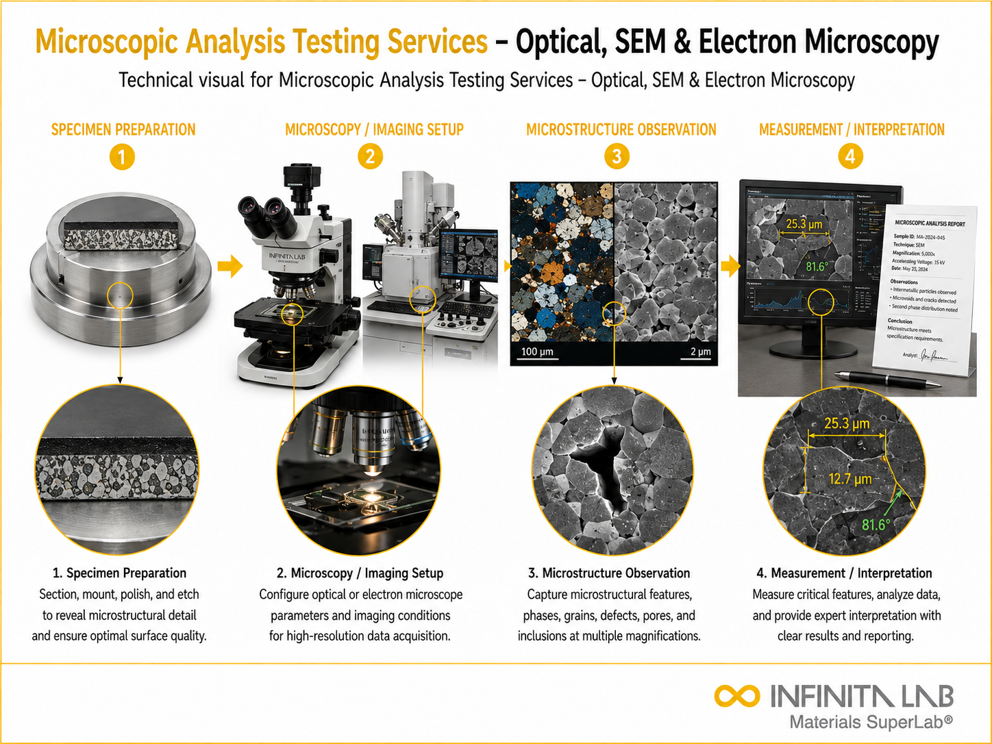
Microscopic Analysis Process
Sample Preparation
Specimen is cleaned, sectioned, mounted, and polished for analysis.
1Surface Conditioning
Etching or coating is applied if required to enhance structural visibility.
2Imaging Observation
Sample is examined under optical or electron microscope at required magnification.
3Data Interpretation
Micrographs are analyzed to identify structure, defects, and material characteristics.
4Microscopic Analysis Technical Specifications
| Parameter | Details |
|---|---|
| Method | Optical and electron beam imaging techniques |
| Measurement Type | Microstructure, morphology, and defect analysis |
| Sample Type | Metals, polymers, ceramics, biological, and semiconductor materials |
| Loading Type | Non-destructive or minimal preparation analysis |
| Units | µm, nm, magnification (×), pixel scale |
| Resolution Range | Micrometer to nanometer scale depending on technique |
| Magnification Range | 10× to >1,000,000× (instrument dependent) |


Instrumentation Used for Testing
- Optical microscope (bright field, dark field, polarized)
- Scanning Electron Microscope (SEM)
- Transmission Electron Microscope (TEM)
- Sample preparation tools (microtome, polisher, etching systems)
- Imaging and analysis software
Results and Deliverables
- High-resolution micrographs of material structure
- Grain size and phase distribution analysis
- Defect identification and classification report
- Surface morphology and texture evaluation
- Failure analysis and documentation report
Frequently Asked Questions
Microscopic analysis identifies defect origin by examining morphology, crack propagation patterns, and surface deformation characteristics. Manufacturing defects often show uniform distribution or process-related signatures, while service-induced damage exhibits directional stress patterns, fatigue striations, corrosion effects, or wear marks formed during operational loading.
Sample preparation is critical because improper cutting, polishing, or etching can introduce artifacts that distort true microstructural features. High-quality preparation ensures accurate representation of grain boundaries, phases, and defects, enabling reliable interpretation and preventing misidentification of structural anomalies.
Grain size is measured using calibrated micrographs and standardized comparison methods such as intercept or planimetric techniques. These measurements help quantify material strength relationships, as smaller grain sizes generally improve mechanical properties like hardness and yield strength.
Contrast enhancement improves visibility of microstructural features that are otherwise indistinguishable. Techniques like etching, staining, or electron beam adjustments highlight phase boundaries, defects, and compositional variations, enabling precise structural interpretation and accurate defect detection.
Electron microscopy offers significantly higher magnification and resolution, enabling visualization of nanoscale features such as dislocations, precipitates, and atomic-level structures. Unlike optical microscopy, it reveals internal and surface details beyond the diffraction limits of visible light.
Why Choose Infinita Lab for Advanced Materials Testing and Characterization?
At the core of this breadth is our network of 2,000+ accredited laboratories across the USA, offering access to over 10,000 testing methods and analytical services. From advanced materials characterization (SEM, TEM, RBS, XPS) to mechanical, chemical, environmental, biological, and standardized ASTM/ISO-compliant testing, we deliver unmatched flexibility, specialization, and scale. You are never limited by geography, facility, or methodology — Infinita Lab connects you to the right expertise and testing solution, every time.

Looking for a Trusted Partner for Accurate and Reliable Testing Services?
Send query us at hello@infinitlab.com or call us at (888) 878-3090 to learn more about our services and how we can support you.


Request a Quote
Submit your material details and receive testing procedures, pricing, and turnaround time within 24 hours.
 Quick Turnaround and Hasslefree process
 Confidentiality Guarantee
 Free, No-obligation Consultation
 100% Customer Satisfaction
