Optical Emission Spectroscopy (OES) Testing Laboratory Services
OES, or optical emission spectroscopy, is a popular analytical method used to ascertain the elemental and chemical composition of a wide variety of metals and alloys.

TRUSTED BY


- Overview
- Scope, Applications, and Benefits
- Test Process
- Specifications
- Instrumentation
- Results and Deliverables
Optical Emission Spectroscopy (OES) Testing Overview
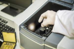
Optical Emission Spectroscopy (OES) is an analytical technique used to determine the elemental composition of metals and alloys by measuring the light emitted from excited atoms. When a high-energy spark or arc is applied, atoms emit characteristic wavelengths that identify and quantify elements present in the sample.
OES provides rapid, accurate, and multi-element analysis, making it essential for material verification, alloy identification, and process control. It is widely used in metallurgy, manufacturing, and quality control applications to ensure materials meet required chemical composition specifications.

Scope, Applications, and Benefits
Scope
OES testing evaluates:
- Elemental composition (% to ppm levels)
- Major, minor, and trace elements (e.g., C, Mn, Cr, Ni, Si)
- Alloy grade identification
- Impurity and contamination detection
Applications
- Steel and alloy manufacturing
- Automotive and aerospace components
- Foundries and casting industries
- Metal fabrication and machining
- Incoming material inspection and verification
Benefits
- Rapid multi-element analysis (results within seconds)
- High accuracy and repeatability
- Minimal sample preparation required
- Suitable for a wide range of metals and alloys
- Enables real-time process control
Optical Emission Spectroscopy (OES) Test Process
Sample Preparation
The sample surface is ground and cleaned to remove oxides and contaminants for accurate excitation.
1Excitation
A spark discharge (~300–500 Hz, high voltage) excites atoms on the sample surface.
2Emission Detection
Emitted light (wavelength range ~120–800 nm) is detected and recorded.
3Data Analysis
Elemental composition is calculated using calibration curves and spectral intensity.
4Optical Emission Spectroscopy (OES) Technical Specifications
| Parameter | Details |
|---|---|
| Standard | ASTM E415, ASTM E1086, ASTM E1251 |
| Applicable Materials | Metals and alloys (steel, aluminum, copper, etc.) |
| Minimum Sample Size | ~5 × 5 mm flat surface |
| Measured Outputs | Elemental composition (% / ppm) |
| Detection Limit | ~1–10 ppm (element dependent) |
| Elements Detected | Up to 20–30 elements simultaneously |
Instrumentation Used for Testing
- Optical emission spectrometer (spark-OES)
- High-voltage spark generator
- Optical system (monochromator/diffraction grating)
- Solid-state detectors (CCD/PMT)
- Sample preparation grinder
- Calibration standards and software
Results and Deliverables
- Quantitative elemental composition (% / ppm)
- Alloy grade identification and verification
- Trace impurity analysis
- Comparative material evaluation
- Input for process control and material selection
Frequently Asked Questions
OES testing is used to determine the elemental composition of metals and alloys. It helps verify material grades, detect impurities, and ensure compliance with required chemical specifications in manufacturing and engineering applications.
OES can detect a wide range of elements including carbon, sulfur, phosphorus, manganese, chromium, nickel, and silicon. It can analyze up to 20–30 elements simultaneously depending on the instrument configuration.
OES can detect elements at very low concentrations, typically in the range of 1–10 ppm depending on the element and instrument sensitivity, making it suitable for trace analysis.
Arc or Spark OES detects the composition of solid materials, while ICP OES is meant for liquid samples.
Proper surface preparation removes oxides and contaminants that can interfere with the spark excitation process. A clean, flat surface ensures accurate and repeatable elemental analysis results.
Why Choose Infinita Lab
for Electron Energy Loss
Spectroscopy (EELS)?
At the core of this breadth is our network of 2,000+ accredited labs in the USA, offering access to over 10,000 test types. From advanced metrology (SEM, TEM, RBS, XPS) to mechanical, dielectric, environmental, and standardized ASTM/ISO testing, we give clients unmatched flexibility, specialization, and scale. You are not limited by geography, facility, or methodology – Infinita connects you to the right testing, every time.
Looking for a trusted partner for Electron Energy Loss Spectroscopy (EELS) Testing?
Send query us at hello@infinitlab.com or call us at (888) 878-3090 to learn more about our services and how we can support you.

Request a Quote
Submit your material details and receive testing procedures, pricing, and turnaround time within 24 hours.
 Quick Turnaround and Hasslefree process

 Confidentiality Guarantee

 Free, No-obligation Consultation

 100% Customer Satisfaction


