
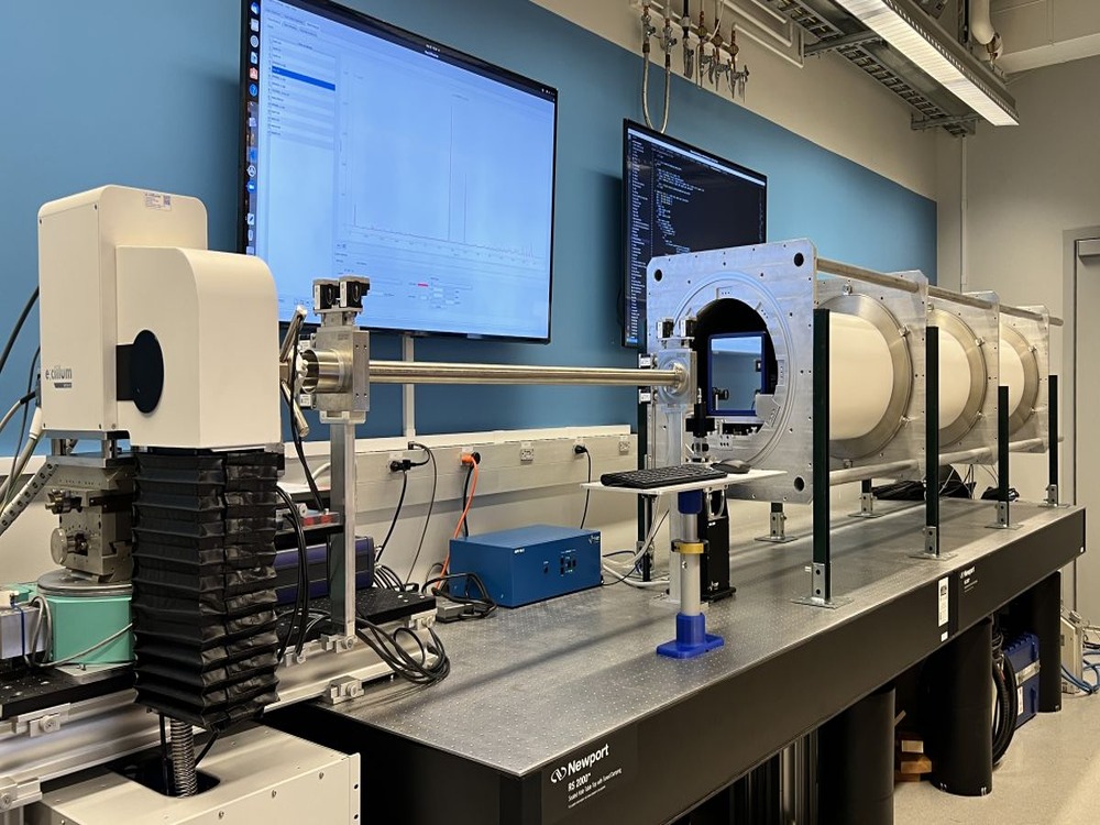
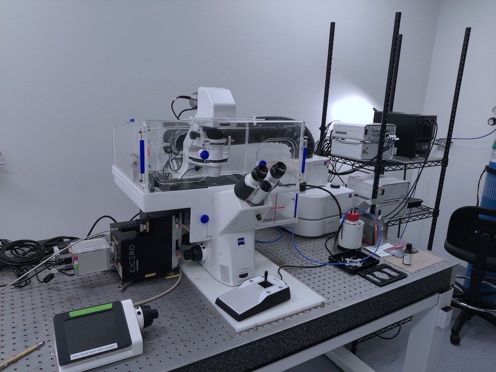
Optical Profilometry
Optical Profilometry (OP) is a non-contact technique to measure surface topography. Through 2D and 3D pictures, an optical profilometer is used to assess a sample's roughness statistics and feature size. Using an optical profilometer, optical profilometry is a non-destructive method of analyzing samples' surface roughness, coating thickness fluctuation, flatness, surface curvature, texture, and thin-film coating stress. Infinita Labs uses cutting-edge technology to provide routine and sophisticated OP analyses.
Optical Profilometry Testing
Optical Profilometry (OP) or White Light Interferometry (WLI) is an interferometric-based non-contact technology for the measurement of surface topography. It is used to measure surface roughness, coating thickness variation, flatness, surface curvature, texture, and thin-film coating stress. It’s a non-destructive and relatively fast method with a wide range of applications. A diamond stylus is scanned on the sample’s surface in a contact mode profilometer while its vertical movement is recorded. In contrast, a non-contact mode profilometer uses a laser or optical beam. The light beam is split with one half directed to the surface and another half to the mirror. When these beams are recombined, the wavelength scale path difference produced by the topography variations causes interference. Contour information is extrapolated from the interpretation of the interference patterns.
An optical profiler can be useful in a wide range of scientific and industrial examination disciplines. It is possible to measure surface forms over wider areas using devices with lesser spatial resolution.
The performance of the profilometer is crucial for an accurate analysis of the surface topography; therefore, the following crucial elements must be taken into account:
- Resolution in space: For various profilometers, the resolution in space varies, notably in the longitudinal and lateral directions. The range of this spatial resolution is determined by the users’ goals, which in turn are determined by the various accuracy levels.
- Field of view: The whole area of the material surface that the profilometer can measure is known as the field of view. This depends on the kind of profiler and its size in order to comprehend the characteristics of the larger area.
- Picture acquisition time: The profilometer’s other key performance indicator is dependent on the measurement technique, the needed image type, image frame rates, and accuracy.
Optical Profilometry Common Uses
- Roughness profile for automotive parts
- Curvature analysis for thin-film stress measurement, adhesion, etc.
- Coating surface characteristics
- Corrosion on the metal surfaces
- Fabric surface morphology
- Imaging of cracks and other surface defects
- Flip chip and other semiconductor packaging flatness and solder bumps
- Measurement of the radius of curvature for optical parts and nanometric surface features2
- Development of high precision die
Optical Profilometry Advantage
- Does not require a vacuum or special chamber
- Can accommodate very large to small samples
- Surface roughness precision in the sub-nanometer range
Optical Profilometry Limitations
- Considerable variation in the surface height hard to measure
- A variation in the refractive index of films can produce erroneous thickness estimations.
Optical Profilometry Industries
- Semiconductors
- Nanotechnology
- Additive Manufacturing
- Advanced Packaging
- Advanced Materials
- Automotive
- LED and Display
- Biomaterials
- Optical Component Manufacturing
More Details
 Metrology Testing Service

- X-ray Fluorescence Spectrometry (XRF)
- Inductively Coupled Plasma Mass Spectrometry – ICP-MS
- Applications of High-Resolution XPS in Battery Research
- Guide to Optical Emission Spectroscopy (OES) Testing
- Liquid Chromatography (LC) Testing
- Time Domain Reflectometry (TDR)
- Micro-Raman Spectroscopy
- Real Time X-ray (RTX)
- View All


3 Easy Steps to Start Testing


Case Studies
In-depth examination of genuine material testing solutions
Dopant and ultra-low concentration elemental analysis using Scanning…

Dopant and ultra-low concentration elemental analysis using Scanning…
EELS analysis of gate and channel is performed on fin field-effect transistors (finFETs). Scanning transmission electron...
Read Case StudyAnalysis of degradation of PVC pipe using Fourier…

Analysis of degradation of PVC pipe using Fourier…
Introduction PVC is the polymer primarily used to make pipes for plumbing, drainage, and electrical conduits....
Read Case StudyNano-scale roughness measurement of Si-wafers by Atomic Force…

Nano-scale roughness measurement of Si-wafers by Atomic Force…
Nano-scale surface roughness is a critical parameter in fabricated thin-films that are used in optics, solar...
Read Case StudyTalk to Our Experts Today!
Submit your contact info and we’ll get back to you within 24 hours
