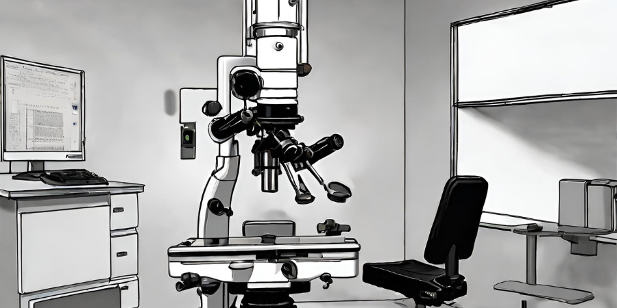
Transmission Electron Microscopy
Transmission Electron Microscopy or TEM is a powerful tool for imaging, spectroscopy, and diffraction analysis. A Transmission Electron Microscope is the most powerful microscopic instrument available and it is used to produce images of electron beam interaction with a sample. TEM performed in our testing labs helps to determine atomic-level structural characteristics of materials required for product design and application.
TRUSTED BY


Precision-driven testing for dimensional accuracy and compliance
- Overview
- Scope, Applications, and Benefits
- Test Process
- Specifications
- Instrumentation
- Results and Deliverables
Overview
TEM, or Transmission Electron Microscopy, is one of the most cutting-edge means of looking into the inner structure and shape of materials at extremely high levels of magnification, down to the nanometer level. This works by shooting a beam of high-energy electrons through an ultra-thin sample, and the interaction with the sample produces detailed images of what’s on the inside.
With the use of TEM, one can view crystal lattices, grain boundaries, dislocations, nanoparticles, and the phase distribution of the sample. This is because the wavelength of electrons is much shorter than the wavelength of light, which makes the resolution of the sample much higher than what’s achieved with light microscopy. This makes it one of the most indispensable tools in the fields of nanotechnology, materials science, and semiconductor physics.

Scope, Applications, and Benefits
Scope
Transmission Electron Microscopy (TEM) is a valuable tool for exploring the inner structure of materials at very high resolution. With TEM, we can look at the microstructure, crystallography, and even the size of particles and defects at the nanometre or even atomic level, and therefore it is extensively used in material science, nanotechnology, and semiconductor research.
Some of the materials on which TEM can be used are:
– Metals and Alloys
– Polymers
– Ceramics
– Nanomaterials
– Thin Films and Coatings
– Semiconductor Materials
– Biological Samples
– Composites
The basic function of TEM is to look at the microstructure, crystallography, and even the size of particles and defects at the nanometre or even the atomic level.
Applications
- Nanomaterial characterization
- Semiconductor device analysis
- Thin film and coating evaluation
- Crystal structure and lattice imaging
- Particle size and morphology analysis
- Defect and dislocation analysis in metals
- Polymer morphology studies
- Failure analysis of advanced materials
Benefits
- Ultra-high spatial resolution imaging
- Atomic and nanometre scale structural analysis
- Precise particle size measurement
- Detailed crystallographic information
- Identification of internal defects and dislocations
- High magnification capability (up to millions of times)
- Supports advanced materials research
- Provides detailed internal structural information
Test Process
Sample Preparation
The sample is thinned to an ultra-thin section (typically <100 nm).
1Electron Beam Generation
A high-energy electron beam is generated and focused using electromagnetic lenses.
2Electron Transmission
The electron beam passes through the thin specimen and interacts with the material’s internal structure.
3Image Formation & Analysis
Transmitted electrons form a magnified image used to analyse crystal structure, defects, and morphology.
4Technical Specifications
| Parameter | Details |
|---|---|
| Resolution | Up to ~0.1 nm (atomic scale) |
| Magnification Range | 10,000× to over 1,000,000× |
| Sample Thickness | Typically <100 nm |
| Imaging Modes | Bright field, dark field, high-resolution TEM |
| Additional Capability | Electron diffraction and elemental analysis (EDS) |
| Applicable Materials | Metals, polymers, ceramics, semiconductors, nanomaterials |
| Output Units | Nanometre-scale images and diffraction patterns |
Instrumentation Used for Testing
- Transmission electron microscope
- Electron gun (thermionic or field emission source)
- Electromagnetic lenses
- Vacuum system
- Sample holder and specimen stage
- CCD/CMOS imaging detectors
- Energy dispersive spectroscopy (EDS) detector
- Image processing and analysis software
Results and Deliverables
- High-resolution TEM images
- Nanostructure and morphology analysis
- Particle size distribution data
- Crystal lattice imaging results
- Electron diffraction pattern analysis
- Defect and dislocation identification
- Material microstructure reports
Why Choose Infinita Lab for Transmission Electron Microscopy?
At the core of this breadth is our network of 2,000+ accredited labs in the USA, offering access to over 10,000 test types. From advanced metrology (SEM, TEM, RBS, XPS) to mechanical, dielectric, environmental, and standardised ASTM/ISO testing, we give clients unmatched flexibility, specialisation, and scale. You’re not limited by geography, facility, or methodology—Infinita connects you to the right testing, every time.
Looking for a trusted partner to achieve your research goals? Schedule a meeting with us, send us a request, or call us at (888) 878-3090 to learn more about our services and how we can support you. Request a Quote
Frequently Asked Questions
Transmission Electron Microscopy is an advanced imaging technique that uses a beam of electrons transmitted through an ultra-thin sample to produce extremely high-resolution images of a material’s internal structure at the nanometre or atomic scale.
TEM can analyze a wide range of materials including metals, alloys, polymers, ceramics, semiconductors, nanomaterials, thin films, coatings, and composite materials.
TEM can achieve extremely high resolution, often up to 0.1 nanometres, allowing researchers to observe crystal lattices, nanoparticles, and atomic arrangements.
The electron beam must pass through the sample to form an image. Therefore, specimens are typically prepared to be less than 100 nm thick so electrons can transmit through the material.
TEM can reveal microstructure, crystal structure, grain boundaries, defects, dislocations, particle size, morphology, and phase distribution within materials.


Request a Quote
Submit your material details and receive testing procedures, pricing, and turnaround time within 24 hours.
 Quick Turnaround and Hasslefree process
 Confidentiality Guarantee
 Free, No-obligation Consultation
 100% Customer Satisfaction
