
X-ray Photoelectron Spectroscopy – XPS
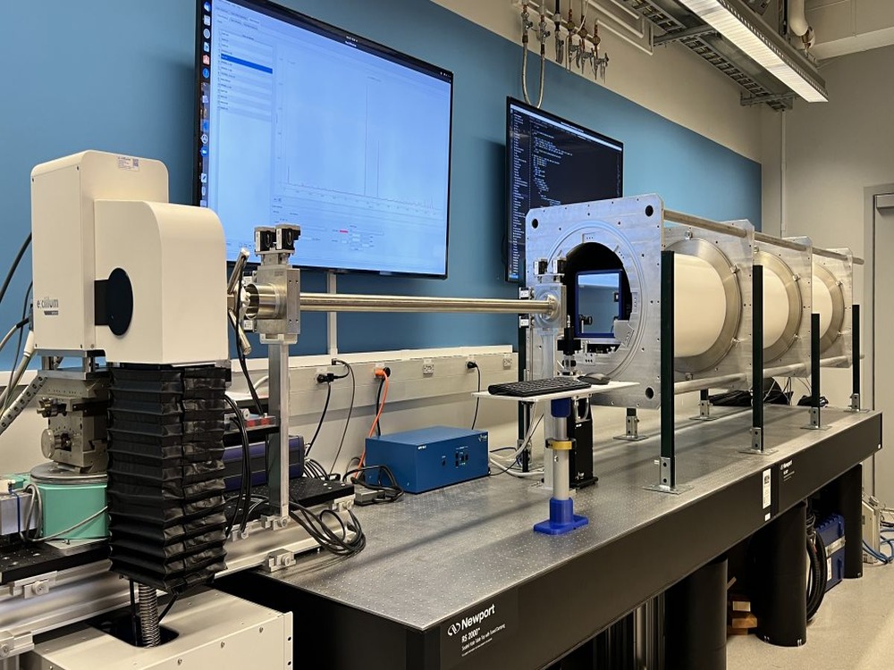
X-ray photoelectron spectroscopy (XPS) is a surface-sensitive elemental analysis technique. It is a powerful tool for determining the elemental and chemical state information of specimen surfaces.
X-ray Photoelectron Spectroscopy Introduction
X-ray photoelectron spectroscopy (XPS) is a surface-sensitive elemental analysis technique. It is a powerful tool for determining the elemental and chemical state information of specimen surfaces. Combined with ion milling, XPS can be applied to depth profiling of thin films, detecting surface contamination of materials, inspecting surface treatments, and other surface characterization in the nanoscale. Its applicability in material characterization is far-reaching from inorganic compounds, metal alloys, polymers, glasses, biomaterials, ion modified materials, coatings, ceramics to semiconductors, etc.
In XPS, a sample is irradiated with the monochromatic x-rays that result in the emission of inner orbital and bonding electrons. The measurement of these electrons binding energies and intensities (from the top 1–10 nm of the sample) allows identification and quantification of the elements on the material’s surface.
X-ray Photoelectron Spectroscopy (XPS) Common Uses
- Determination of the empirical formula of pure materials
- Distinguishing between sulfide and sulfate forms of a sulfur element
- Analysis of the surface composition of fiber-reinforced composite materials
- Quantitative information about graphene, such as the number of layers and identification of impurities
- Determining the differences in oxide layer (SiON, SiO2) thickness between samples
- Quantitative analysis of surface layers generated during the wear process
- Chemical analysis of plasma-treated textiles
- Analysis of stainless steel passivation by determining the corrosion, adhesion, and friction properties
- Investigation of the extent of functionality and specific adsorption or binding of the biomolecules (proteins, enzymes, lipids) onto the various surfaces
X-ray Photoelectron Spectroscopy Advantages
- An effective technique for both conductive and insulating samples
- Provides extensive information such as surface sensitivity; quantifiable elemental and chemical details2
- Ability to perform depth profiling by quantifying matrix-level elements as a function of depth
- Ability to distinguish between oxidations states of the molecules
X-ray Photoelectron Spectroscopy Limitations
- Samples should be compatible with an ultra-high vacuum (UHV) environment; unsuitable for biological samples
- Detection of all elements except H and He
- Identification of the elemental composition in ~ 0.1 atomic percent or 1000ppm
- Typically, the smallest analytical area is ~10 µm
- The low resolution of source radiation (~0.1 – 1.0 eV)
- Many potential artifacts may arise that are often related to the sample preparation
- It takes a long time (½ to 8 hours per sample) to obtain the XPS spectrum
Industries
- Semiconductors
- Electronics
- Chemical Industry
- Thin Films and Coatings
- Tribology
- Advanced Materials
- Biotechnology
- Metal/Steel Industry
- Fiber Composites
- More Details
- Working principle of XPS
- Limitations of XPS
Infinita Lab offers comprehensive X-ray Photoelectron Spectroscopy Testing Services, ensuring precise and reliable results. With a network of accredited material testing laboratories across the USA, Infinita Lab provides nationwide coverage, including 16 office locations, doorstep sample pickup, and expert consultancy for detailed report analysis. Our extensive catalog includes over 2000 material science tests. Our services help industries such as semiconductor, aerospace, medical devices, renewable energy. Trust Infinita Lab for your material testing needs. Visit our website to learn more and schedule your testing services today.
FAQs on X-ray Photoelectron Spectroscopy
It provides qualitative and quantitative information about surface composition, oxidation states, elemental distribution, and chemical bonding environments.
XPS typically analyzes the top 1–10 nanometers of a material’s surface.
XPS measures the kinetic energy of electrons ejected from a material’s surface when irradiated with X-rays. The binding energies of these electrons identify the elements and their chemical states.
 Metrology Testing Service

- High Performance Liquid Chromatography (HPLC)
- X-Ray Diffraction (XRD)
- AI Suited to Industrial Inspection
- Differential Scanning Calorimetry
- X-Ray Diffraction Analysis – XRD
- Liquid Chromatography (LC) Testing
- Liquid Chromatography with Tandem Mass Spectrometry (LC-MS/MS)
- Electrothermal Vaporization ICP Optical Emission Spectroscopy (ETV-ICP-OES)
- View All


3 Easy Steps to Start Testing


Case Studies
In-depth examination of genuine material testing solutions
Dopant and ultra-low concentration elemental analysis using Scanning…

Dopant and ultra-low concentration elemental analysis using Scanning…
EELS analysis of gate and channel is performed on fin field-effect transistors (finFETs). Scanning transmission electron...
Read Case StudyAnalysis of degradation of PVC pipe using Fourier…

Analysis of degradation of PVC pipe using Fourier…
Introduction PVC is the polymer primarily used to make pipes for plumbing, drainage, and electrical conduits....
Read Case StudyNano-scale roughness measurement of Si-wafers by Atomic Force…

Nano-scale roughness measurement of Si-wafers by Atomic Force…
Nano-scale surface roughness is a critical parameter in fabricated thin-films that are used in optics, solar...
Read Case StudyTalk to Our Experts Today!
Submit your contact info and we’ll get back to you within 24 hours
