Electron Backscatter Diffraction (EBSD)
Electron Back-scatter Diffraction (EBSD) is an advanced analytical technique used to study the microstructure and crystallographic properties of materials. It is commonly used in materials science, metallurgy, geology, and other fields to investigate the crystal structure, grain orientation, and texture of materials.

TRUSTED BY


Precision-driven testing for dimensional accuracy and compliance
- Overview
- Scope, Applications, and Benefits
- Test Process
- Specifications
- Instrumentation
- Results and Deliverables
Overview
Electron Back Scatter Diffraction (EBSD) is a sophisticated technique to investigate the microstructure of a material that is crystalline in nature. When a tilted crystal is placed in front of an SEM and an electron beam is focused on its surface, which is polished, it reveals information about how the atoms are arranged, what phases are present, and how they are arranged in a particular pattern of grains.
When the electrons are incident on the crystal, back-scattered electrons are emitted, and this is known as a Kikuchi pattern. An EBSD detector is specifically designed to detect this pattern, and from this information, it is possible to deduce information about the crystals and how they are arranged in a particular material. This technique is a mainstay in materials science, metallurgy, and semiconductor engineering.

Scope, Applications, and Benefits
Scope
Electron Backscatter Diffraction (EBSD) is a characterisation technique used to investigate the microstructure of materials. It is typically used in conjunction with a scanning electron microscope (SEM) and helps us take a peek at the material’s microstructure, including grain structure, orientation, and phase composition, among others.
This technique of EBSD can be used on many kinds of crystalline materials, such as:
– Metals and alloys
– Ceramics
– Semiconductors
– Minerals
– Thin films
– Coatings
This helps us gain crucial information on how the material will behave and how it will react during the process.
Applications
- Microstructure characterisation of metals and alloys
- Grain size and grain boundary analysis
- Crystallographic texture analysis
- Phase identification in multiphase materials
- Failure analysis and fracture studies
- Semiconductor material characterisation
- Thin film and coating evaluation
- Additive manufacturing material studies
Benefits
- Provides detailed crystallographic information
- High spatial resolution microstructure analysis
- Accurate grain orientation mapping
- Identifies multiple crystalline phases
- Helps understand deformation and recrystallisation mechanisms
- Supports failure analysis and materials development
- Non-destructive surface analysis with minimal material removal
- Enhances process optimisation and quality control
Test Process
Sample Preparation
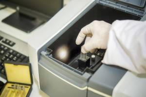
The specimen surface is polished to obtain a smooth, damage-free surface suitable for EBSD analysis.
1Specimen Mounting & Tilting
The sample is mounted in the SEM chamber and tilted to about 70° for optimal backscattered electron detection.
2Electron Beam Interaction
A focused electron beam scans the surface and interacts with the crystal lattice, generating Kikuchi diffraction patterns.
3Pattern Detection & Analysis
Diffraction patterns are captured and analysed to produce orientation, grain boundary, and phase maps.
4Technical Specifications
| Parameter | Details |
|---|---|
| Instrument Platform | Scanning Electron Microscope (SEM) |
| Typical Sample Tilt | Approximately 70° |
| Applicable Materials | Crystalline metals, alloys, ceramics, semiconductors, and minerals |
| Measured Properties | Crystal orientation, grain size, grain boundaries, phase identification, texture |
| Spatial Resolution | Typically 20 nm to 100 nm depending on material and SEM configuration |
| Output Data | Orientation maps, phase maps, grain boundary maps, pole figures |
Instrumentation Used for Testing
- Scanning Electron Microscope (SEM)
- EBSD detector and phosphor screen
- High-resolution CCD or CMOS camera
- Sample preparation and polishing equipment
- Ion polishing system (optional)
- Crystallographic analysis software
- Data processing and mapping software
Results and Deliverables
- Crystallographic orientation maps
- Grain size distribution analysis
- Grain boundary characterisation
- Phase identification and distribution maps
- Texture and pole figure analysis
- Microstructure characterisation reports
- Comparative microstructural analysis
Why Choose Infinita Lab for Electron Backscatter Diffraction(EBSD)?
With Infinita Lab (www.infinitalab.com), you are guaranteed a Nationwide Network of Accredited Laboratories spread across the USA, the best Consultants from around the world, Convenient Sample Pick-Up and Delivery, and Fast Turnaround Time.
Our team understands the stakes and subtleties of every test. Whether you’re validating a new Product, de-risking a prototype, or navigating complex compliance requirements, our specialists guide the process with rigor and clarity.
Looking for a trusted partner to achieve your research goals? Schedule a meeting with us, send us a request, or call us at (888) 878-3090 to learn more about our services and how we can support you. Request a Quote
Frequently Asked Questions
It is a powerful and versatile analytical technique widely used for detailed crystallographic analysis in materials science, geology, and engineering.
EBSD is primarily used to analyze the crystallographic structure of materials. It helps determine grain orientation, phase identification, texture analysis, and microstructural characterization.
EBSD directs an electron beam onto a tilted, polished sample within a scanning electron microscope (SEM). The electron beam's interaction with the sample surface causes electrons to scatter, forming diffraction patterns. A detector captures and analyzes these patterns to reveal information about the material's crystal structure, grain orientation, and phase.
EBSD is most effective for analyzing crystalline materials, including metals, ceramics, and minerals.
While EBSD is a powerful technique, it has limitations, including surface sensitivity, limited spatial resolution compared to other methods like TEM, and a shallow penetration depth.
Case Studies
In-depth examination of genuine material testing solutions
Dopant and Ultra-Low Concentration Elemental Analysis Using STEM…
Introduction to STEM-EELS for Elemental Analysis Scanning Transmission Electron Microscopy (STEM) combined with Electron Energy Loss...
Read Case StudyAnalysis of PVC Pipe Degradation Using FTIR Spectroscopy
PVC Pipe in Infrastructure — and Why Degradation Matters Polyvinyl chloride (PVC) pressure pipe is one...
Read Case StudyNano-scale roughness measurement of Si-wafers by Atomic Force…
Nano-scale surface roughness is a critical parameter in fabricated thin-films that are used in optics, solar...
Read Case Study
Request a Quote
Submit your material details and receive testing procedures, pricing, and turnaround time within 24 hours.
 Quick Turnaround and Hasslefree process

 Confidentiality Guarantee

 Free, No-obligation Consultation

 100% Customer Satisfaction


