
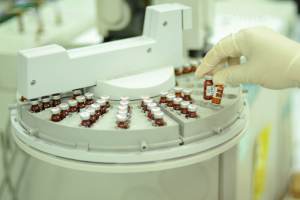
The cross-sectional or micro-sectional analysis is a destructive analysis that measures the quality of the manufactured board. It's basically an interconnection defect analysis process that detects and verifies what went wrong inside the PCB. This is an integral part of the PCB manufacturing process.
There are a few procedures you may follow when performing a PCB (Printed Circuit Board) cross-section analysis to look for hidden flaws. Here is a general rule of thumb:
To obtain the PCB cross-section, carefully choose the area of the PCB where you think the hidden problem might be. In order to produce a cross-sectional sample without causing more harm, use the proper cutting equipment or techniques.
Cross-sectional analysis samples should be cleaned to get rid of any pollutants that can affect the analysis. Utilizing cleaners or solvents safe for PCB materials may be required to do this. Check to see that the sample is dry before continuing.
Removal of protective encapsulation: If the fault is thought to be hidden beneath the conformal coating or protective encapsulation, these layers should be carefully removed using the appropriate techniques, such as chemical stripping or mechanical removal. Be careful not to harm the supporting structures.
The exposed cross-section sample should be polished to create a smooth surface suitable for microscope investigation. To attain the desired surface polish, start with a coarse abrasive substance and gradually work your way up to finer grit sizes. Between each polishing stage, thoroughly clean and rinse the sample.
Examine the cross-section sample under a microscope, such as an optical microscope or a scanning electron microscope (SEM). High-resolution imaging of the sample and the detection of any flaws or anomalies are made possible by this examination.
Analysis and defect detection: Use a microscope to look at the cross-section sample and look for any hidden flaws. Keep an eye out for anomalies that could point to a flaw in the PCB structure or manufacturing process, such as delamination, cracks, voids, or other irregularities.
Documentation and imaging: Take pictures or videos of the detected flaws for your records. Further analysis, quality assurance, or contact with other stakeholders may benefit from this documentation.
Additional testing: You might need to do additional testing or analysis to identify the cause of the discovered defect, depending on its type. Techniques like X-ray inspection, electrical testing, or chemical analysis might be used for this.
Remedial action: Once problems have been located and their underlying causes established, remedial action can be conducted. To prevent the occurrence of the same errors in the future, this may need rework, repairs, or changing the production procedure.
It’s crucial to remember that performing a PCB cross-sectional study calls for knowledge and specialized tools. If you are unfamiliar with the procedure, it may be best to seek advice from a qualified PCB engineer or failure analysis lab to assure correct results.
Liquid Chromatography-Mass Spectroscopy Liquid Chromatography-Mass Spectroscopy (LC-MS) is an analytical technique that allows the separation, identification, and quantification of the...
Read Article ➙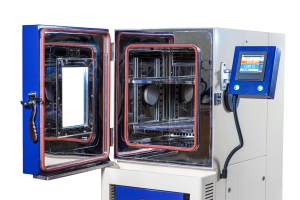
Highly Accelerated Stress Test - HAST Testing Services A highly accelerated stress test (HAST) is an essential part of environmental...
Read Article ➙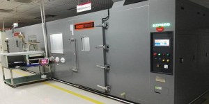
Introduction Accelerated aging in product testing is a methodology that simulates the long-term effects of environmental factors on a product...
Read Article ➙In-depth examination of genuine material testing solutions

EELS analysis of gate and channel is performed on fin field-effect transistors (finFETs). Scanning transmission electron...
Read Case Study
Introduction PVC is the polymer primarily used to make pipes for plumbing, drainage, and electrical conduits....
Read Case Study
Nano-scale surface roughness is a critical parameter in fabricated thin-films that are used in optics, solar...
Read Case StudySubmit your contact info and we’ll get back to you within 24 hours
