
Finding the primary reason for failures in semiconductor devices requires a vital technique called integrated circuit (IC) failure analysis. The failure processes must be analyzed and diagnosed using a variety of techniques and methodologies. As technology has advanced and semiconductor devices have become more complicated, various cutting-edge trends in IC failure analysis have developed in recent years.
The following are some noteworthy IC failure analysis trends:
Modern Packaging Techniques: IC failure analysis now faces new difficulties as a result of the emergence of advanced packaging technologies, including system-in-package (SiP), wafer-level packaging (WLP), and 3D packaging. These packaging strategies combine several components into a single unit, making it more challenging to identify and fix problems. In order to address the distinctive failure modes linked to various packaging technologies, cutting-edge methods and tools are being created.
High-Resolution Imaging: To properly image and characterize IC architectures at the submicron and nanoscale levels, failure analysis is required. IC failure analysis is becoming more and more dependent on high-resolution imaging methods, including focused ion beam (FIB) microscopy, transmission electron microscopy, and scanning electron microscopy (SEM). Higher resolution and quicker acquisition speeds, two improvements in these imaging techniques, allow for more precise and effective failure location and analysis.
Fault Isolation and Localization: Finding the precise location of a fault gets more difficult as semiconductor devices continue to get smaller and more complex. Fault isolation methods like electron beam-induced current (EBIC), laser voltage probing (LVP), and emission microscopy are used to find faults and figure out how they happen in ICs. Effective failure analysis and yield enhancement require these methods.
Circuit Editing and Nanoprobing: Nanoprobing is a method that enables precise electrical measurements on individual transistors and interconnects inside an integrated circuit (IC). It facilitates the detection of electrical defects and the comprehension of device behavior at the circuit level. Circuit editing methods physically alter IC components in order to fix or improve circuits for analysis or debugging. For precise fault location and diagnosis in IC failure analysis, these techniques are becoming more and more important.
Big Data and Artificial Intelligence (AI): There is an increasing demand for data analysis and interpretation tools due to the complexity and volume of data collected during IC failure analysis. Data from failure analysis is being analyzed using big data analytics and AI techniques to spot patterns and gain useful insights. Machine learning algorithms can aid in the classification of failure signatures and the prediction of failure mechanisms, which will increase the efficacy and precision of failure analysis procedures.
Reliability and Failure Prediction: To guarantee the high quality and endurance of semiconductor devices, reliability evaluation and failure prediction are essential. The dependability of ICs is assessed using methods such as accelerated life testing, stress testing, and thermal analysis under a variety of operating conditions. Failure analysis is essential for spotting possible problems with reliability and for optimizing device designs to increase overall product reliability.
These patterns show how IC failure analysis is still working to keep up with advances in semiconductor technology. Engineers and researchers may efficiently identify and fix issues by utilizing cutting-edge techniques and procedures, which will increase semiconductor sector product quality, yield, and dependability.
Video 01: Integrated circuit failure analysis

Liquid Chromatography-Mass Spectroscopy Liquid Chromatography-Mass Spectroscopy (LC-MS) is an analytical technique that allows the separation, identification, and quantification of the...
Read Article ➙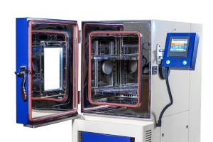
Highly Accelerated Stress Test - HAST Testing Services A highly accelerated stress test (HAST) is an essential part of environmental...
Read Article ➙
Introduction Accelerated aging in product testing is a methodology that simulates the long-term effects of environmental factors on a product...
Read Article ➙In-depth examination of genuine material testing solutions

EELS analysis of gate and channel is performed on fin field-effect transistors (finFETs). Scanning transmission electron...
Read Case Study
Introduction PVC is the polymer primarily used to make pipes for plumbing, drainage, and electrical conduits....
Read Case Study
Nano-scale surface roughness is a critical parameter in fabricated thin-films that are used in optics, solar...
Read Case StudySubmit your contact info and we’ll get back to you within 24 hours
