
Utilising voltage alteration tools, failure analysis of electronic circuits entails changing the voltage levels applied to the circuit in order to detect and pinpoint the primary cause of failure. The process of troubleshooting and repair is aided by the ability to notice changes in behaviour, spot defective parts, and target circuitry sections that may be the source of the failure by selectively adjusting the voltage levels.

Electronic circuits require a range of methods to do a thorough failure analysis, many of which are geared towards isolating a defect to a single point in the intricate network of metal and polysilicon that constitutes an integrated circuit. To collect data regarding the part’s condition, such as taking heat readings or gathering light emitted from the circuit, the great majority of these tools require the failing device to be electrically biased in its failing state. These resources are frequently adequate to identify a flaw; other faults, however, do not readily manifest themselves under these techniques of study. In these circumstances, it is frequently required to utilize a distinct kind of tool, which modifies the device using an external stimulus before measuring the device’s response.
Most of these voltage-altering devices use lasers as their external stimulation. The ability to accurately direct energy onto a specific area of the electrical circuit thanks to the laser’s finely focused beam makes failure analysis easier by enabling the user to identify even the smallest flaws. The electrical bias conditions (the voltage and current provided to the device) are closely watched while the laser is scanned across the die’s surface to look for flaws. According to the sort of defect that is present, a change in the bias imparted to the part can be seen as the laser passes over it. A comprehensive image depicting the exact position of a defect can then be produced for an analyst by mapping this alteration onto an image of the device.
This approach to electronic circuit failure investigation will deliver various data sets depending on the kind of laser used. The use of an infrared laser with photon energy below the silicon bandgap of 1.12 electron volts frequently results in thermal changes on the die; the heating and subsequent relaxation cooling of the semiconductor and metal components of the circuit create resistance changes that, while negligible on a healthy device, are easily mapped on a defective one. The opposite of a thermal laser is a laser that has energy at or above the bandgap of silicon. It is used to create free carriers in the semiconductor materials of the device, increasing the circuit’s current, which can then be measured and compared to a defect-free unit to find where the problem is.
These voltage alteration techniques have the advantage that they can be used to conduct failure analysis on electrical circuits that are a little more atypical than the average IC. In fact, in a pinch, all you need is a laser pointer and a steady hand to make a field-efficient technique to test photovoltaic systems in this way!
Video 01: Integrated circuit failure analysis

Liquid Chromatography-Mass Spectroscopy Liquid Chromatography-Mass Spectroscopy (LC-MS) is an analytical technique that allows the separation, identification, and quantification of the...
Read Article ➙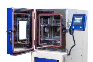
Highly Accelerated Stress Test - HAST Testing Services A highly accelerated stress test (HAST) is an essential part of environmental...
Read Article ➙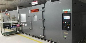
Introduction Accelerated aging in product testing is a methodology that simulates the long-term effects of environmental factors on a product...
Read Article ➙In-depth examination of genuine material testing solutions

EELS analysis of gate and channel is performed on fin field-effect transistors (finFETs). Scanning transmission electron...
Read Case Study
Introduction PVC is the polymer primarily used to make pipes for plumbing, drainage, and electrical conduits....
Read Case Study
Nano-scale surface roughness is a critical parameter in fabricated thin-films that are used in optics, solar...
Read Case StudySubmit your contact info and we’ll get back to you within 24 hours
