
Fluorescence microscopy, also referred to as emission microscopy, is a method used in imaging and microscopy that employs a less rigorous method of fluorescence analysis. It makes use of fluorescent probes or dyes that, in response to a specific light source, emit light of a particular wavelength.
Emission microscopy operates as follows:
A successful failure analysis involves isolating a single flaw from numerous circuits, such as a leaky gate or overdriven transistor, to target the most damaging parts. While thermal imaging and heat-sensitive techniques can be effective in isolating areas, they may not be sufficient in certain situations. Instead, an alternative strategy involves thoroughly understanding a device by comparing its distinctive signature to those of devices that are functioning well. Emission microscopy is a useful technique for characterizing devices and providing a comprehensive representation of various failure types.
Emission microscopy, also known as light emission microscopy or photoemission microscopy, uses a high-gain camera to detect the small amounts of light emitted by semiconductor devices and flaws. The item is placed in a black microscope cage and electrically biased to simulate a failing condition. The camera system takes pictures and integrates data over hours. After integration, the system superimposes an image of the failed chip with a map of the emitted light, revealing regions of intense photoemission with contrasting bursts of color. Photoemission can be caused by factors like overstress, gate oxide pinholes, and even malfunctioning semiconductor devices. Emission microscopy is valuable for creating functional maps of devices, despite potential false positives.
Emission microscopy is a technique that can locate defects in devices like ESD protection diodes and can be used to compare failing units to known good devices. By examining a working device in its typical operational state, analysts can create a benchmark against which to compare the failed device. Emission microscopy analysis of faulty components is reduced to a game of “find the differences,” with broken transistors and damaged diffusions replacing the usual frivolous fare of tulips or buttons.
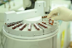
Emission microscopy is typically carried out after a part has undergone chemical decapsulation, where the plastic encapsulant material is removed from the microchip. Junctions and transistors are often sources of photoemission, which are buried beneath densely packed metal layers in semiconductor devices. However, the emission microscope camera’s sensitivity to short-wave infrared light allows for imaging through the rear side of the device, circumventing the problem of interfering metal layers. The device is thinned and polished to a mirror finish, and when used with an infrared illumination source, the emission microscope can produce images similar to conventional images. The camera collects some of the photoemission that passes all the way through the substrate. The dense metallization that conceals the camera’s emission sites can be removed by imaging from the back side, leaving only the semi-translucent silicon substrate between the active layer and the camera’s view.
Read more: Thermal Emission Microscopy – A Useful Failure Analysis Tool
Finding the causes of a malfunctioning semiconductor device’s faults can be done with the use of emission microscopy. But it’s vital to keep in mind that the emission microscope can only produce a picture; it falls to a skilled failure analyst to take that picture and turn it into information that may be utilized to identify flaws in a broken device.
Liquid Chromatography-Mass Spectroscopy Liquid Chromatography-Mass Spectroscopy (LC-MS) is an analytical technique that allows the separation, identification, and quantification of the...
Read Article ➙
Highly Accelerated Stress Test - HAST Testing Services A highly accelerated stress test (HAST) is an essential part of environmental...
Read Article ➙
Introduction Accelerated aging in product testing is a methodology that simulates the long-term effects of environmental factors on a product...
Read Article ➙In-depth examination of genuine material testing solutions

EELS analysis of gate and channel is performed on fin field-effect transistors (finFETs). Scanning transmission electron...
Read Case Study
Introduction PVC is the polymer primarily used to make pipes for plumbing, drainage, and electrical conduits....
Read Case Study
Nano-scale surface roughness is a critical parameter in fabricated thin-films that are used in optics, solar...
Read Case StudySubmit your contact info and we’ll get back to you within 24 hours
