
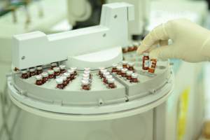
Investigation and root cause analysis are key components of capacitor failure investigations. There are numerous factors that can cause capacitor failures, including aging, electrical stress, manufacturing flaws, or environmental factors.

Electron microscopy is a vital tool for examining various types of flaws, including molten silicon and broken metallization. It can also be used as an isolation technique, altering the electron beam’s interaction with a sample by applying a charge consciously. This method, known as “charge contrast” or “voltage contrast“, is useful for identifying specific anomalies, particularly those leading to open circuits. Some flaws might not require additional setup, and an analyst might be able to spot a flaw just by looking at the passive charge contrast the electron beam produces.
A capacitor is a crucial part of any electronic assembly, and a broken capacitor often results in a system failing completely. Capacitor failure analysis brings up specific issues that demand corresponding solutions. The ultimate goal of capacitor failure analysis is to determine the fundamental cause of failure or whether the incorrect operation is due to manufacturing flaws, end-user abuse, or other causes.
The first step in capacitor failure analysis is finding where an analyst should start looking for a failure, similar to an integrated circuit. Failing capacitors rarely give obvious signs of malfunctioning, but with a little imagination, the same set of tools an analyst employs to find flaws in an integrated circuit can also be used to analyze a capacitor.
Leakage between the two electrodes of a capacitor due to a damaged dielectric is the most frequent cause of failure. A multi-layer ceramic capacitor, also known as a chip cap, employs a ceramic substance made of tiny particles of different materials mixed together to obtain a specific set of properties. The most frequent failure with this type of capacitor is interior layer cracking or delamination.
Acoustic microscopes can be used to find damaged dielectrics in capacitors, but they do not always proceed in the same way as analyzing a packaged IC.
The C-Mode image and A-Scans are two main acoustic approaches for assessing the condition of a package in a packaged IC. The C-Mode image details interfaces within the package, while A-Scans compare reflected acoustic waves at various sites. However, the C-Scan can only look at one interface at a time, making it not the best method for studying the entire device. The best method for a ceramic capacitor is the B-Scan, which produces cross-sectional images of the entire component thickness. This method helps identify damaged dielectrics and their relative locations within the capacitor.
Thermal imaging and other techniques can also be used to confirm a failure a second time by connecting an electrical signature to a physical flaw found when the device is taken apart or cut open. Capacitor failure analysis is a difficult but worthwhile task, even if the outcome is simply an increase in product reliability rather than preventing an uncontrollable inferno.
Liquid Chromatography-Mass Spectroscopy Liquid Chromatography-Mass Spectroscopy (LC-MS) is an analytical technique that allows the separation, identification, and quantification of the...
Read Article ➙
Highly Accelerated Stress Test - HAST Testing Services A highly accelerated stress test (HAST) is an essential part of environmental...
Read Article ➙
Introduction Accelerated aging in product testing is a methodology that simulates the long-term effects of environmental factors on a product...
Read Article ➙In-depth examination of genuine material testing solutions

EELS analysis of gate and channel is performed on fin field-effect transistors (finFETs). Scanning transmission electron...
Read Case Study
Introduction PVC is the polymer primarily used to make pipes for plumbing, drainage, and electrical conduits....
Read Case Study
Nano-scale surface roughness is a critical parameter in fabricated thin-films that are used in optics, solar...
Read Case StudySubmit your contact info and we’ll get back to you within 24 hours
