Nano-scale roughness measurement of Si-wafers by Atomic Force Microscopy (AFM)

Fabricated thin films require smooth nano-scale surfaces for effective usage. Infinitalab offers different types of high precision surface measurements using AFM and other cutting-edge techniques to monitor surface roughness on fabricated thin film substrates.

Last Updated: August 26th, 2024 First Published :
banner
  

Nano-scale surface roughness is a critical parameter in fabricated thin-films that are used in optics, solar cells, data storage, and semiconductor electronics. One such example is for optimizing growth conditions to achieve atomically smooth films on Si-wafers. AFM is used for high-precision surface measurements to monitor surface roughness on substrates. The thicknesses of these layers are in the range of a few to 50 nm. Minute variations in growth conditions can influence the uniformity of these layers compromising the component’s performance.

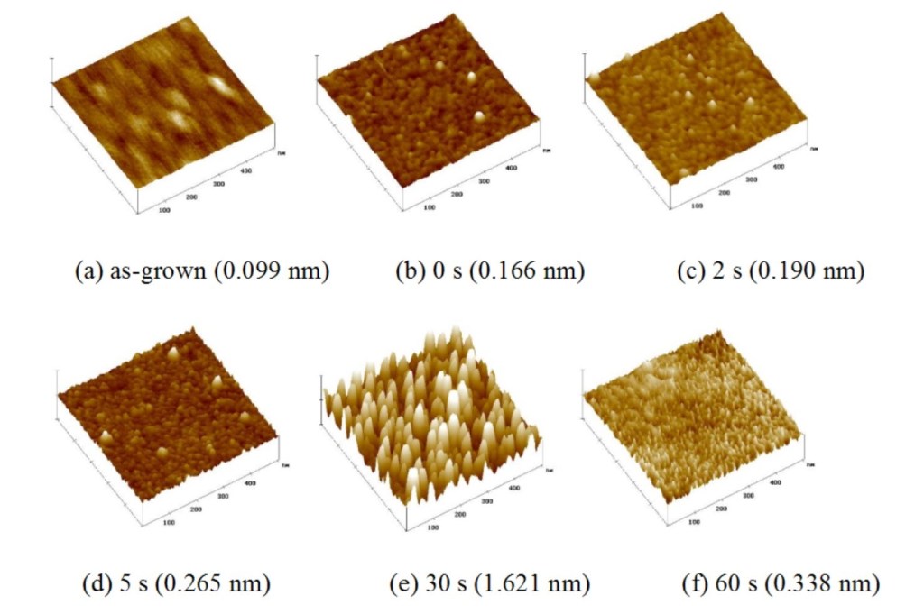
In the below example, AFM imaging is used to assess pre-treatment times and their effect on surface roughness. Figure 1 shows the root mean square (RMS) surface roughness of Si-wafers with varying pre-treatment durations. As seen here, AFM can show topographical variations in the range of 10-1 nm with three-dimensional spatial resolution.

Reference:

[1] Kim, C., Kim, Y., Ryu, H., Kang, J., Kim, S., Min, B., & Lee, H. (2007). Wall-Controlled Growth of CNTs for X-ray Electron Sources. Journal of the Korean Physical Society, 51, 193-197.

Case Studies

In-depth examination of genuine material testing solutions

Dopant and Ultra-Low Concentration Elemental Analysis Using STEM…

banner

Dopant and Ultra-Low Concentration Elemental Analysis Using STEM…

Introduction to STEM-EELS for Elemental Analysis Scanning Transmission Electron Microscopy (STEM) combined with Electron Energy Loss...

Read Case Study

Analysis of PVC Pipe Degradation Using FTIR Spectroscopy

Fourier Transform Infrared Spectroscopy (FTIR)

Analysis of PVC Pipe Degradation Using FTIR Spectroscopy

PVC Pipe in Infrastructure — and Why Degradation Matters Polyvinyl chloride (PVC) pressure pipe is one...

Read Case Study

Nano-scale roughness measurement of Si-wafers by Atomic Force…

banner

Nano-scale roughness measurement of Si-wafers by Atomic Force…

Nano-scale surface roughness is a critical parameter in fabricated thin-films that are used in optics, solar...

Read Case Study

Looking for Material Testing?

We have already delivered 20,000+ Material Test results to top companies

    Home / Case Studies / Nano-scale roughness measurement of Si-wafers by Atomic Force Microscopy (AFM)

    Discover more from Infinita Lab

    Subscribe now to keep reading and get access to the full archive.

    Continue reading

    ×

    Talk to an Expert

      Connect Instantly

      (888) 878-3090
      Ensure Quality with the Widest Network of Accredited Labs
      • ddd
        Quick Turnaround and Hasslefree process
      • ddd
        Confidentiality Guarantee
      • ddd
        Free, No-obligation Consultation
      • ddd
        100% Customer Satisfaction

        ddd

        Start Material Testing