


Voltage Alteration Failure Analysis
Utilising voltage alteration tools, failure analysis of electronic circuits entails changing the voltage levels applied to the circuit in order to detect and pinpoint the primary cause of failure. The process of troubleshooting and repair is aided by the ability to notice changes in behaviour, spot defective parts, and target circuitry sections that may be the source of the failure by selectively adjusting the voltage levels.
TRUSTED BY


Voltage Alteration Failure Analysis
- Overview
- Scope, Applications, and Benefits
- Test Process
- Specifications
- Instrumentation
- Results and Deliverables
Voltage Alteration Failure Analysis Overview
Voltage alteration failure analysis investigates electronic components and assemblies that have failed or degraded as a result of exposure to voltage conditions outside their design specifications. This includes overvoltage events, electrostatic discharge (ESD), electrical overstress (EOS), voltage transients, reverse polarity, and sustained operation at voltages that exceed rated limits. These failure modes are among the most common causes of electronic component returns, field failures, and reliability escapes in consumer electronics, automotive, industrial, and aerospace applications.
The distinction between ESD and EOS failures matters because the corrective actions are different. ESD damage is caused by a very brief, high-voltage, low-energy discharge -typically from a human body or charged object -that creates a localized dielectric breakdown or junction damage that is often microscopic in size. EOS damage is caused by longer-duration overvoltage or overcurrent events that generate excessive power dissipation in the device, causing metal melting, oxide rupture, and larger-area thermal damage. A junction that shows a broad melted metal signature was damaged by EOS; one with a pinhole through the gate oxide was damaged by ESD. Getting that distinction right determines whether the corrective action is improved ESD handling or a circuit design review.
At Infinita Lab, we coordinate voltage alteration failure analysis through our network of accredited labs covering the full range of electrical characterization and physical analysis tools needed to identify voltage-related damage mechanisms in semiconductor components, discrete devices, connectors, and PCB assemblies.

Voltage Alteration Failure Analysis Scope, Applications, and Benefits
Scope
Voltage alteration failure analysis covers failure investigation for electronic components and assemblies damaged by overvoltage, ESD, EOS, voltage transients, reverse bias, and latch-up. Analysis workflow includes electrical characterization to define and reproduce the failure signature, non-destructive inspection by X-ray and scanning acoustic microscopy, physical decapsulation and die access, optical and SEM inspection of the die surface and metallization, EDS elemental analysis for burn and melt signatures, and FIB cross-sectioning to access gate oxides, junctions, and metal interconnects where internal dielectric or junction damage is suspected. Failure mechanism classification covers ESD (HBM, CDM, MM), EOS (forward and reverse bias overstress), latch-up, and secondary breakdown.
Applications
- ESD damage investigation for field returns from consumer electronics, automotive, and industrial equipment
- EOS failure analysis for components returned from production assembly or field service
- Transient overvoltage damage assessment in power electronics and motor drive circuits
- Reverse polarity failure investigation in battery-powered devices and automotive modules
- Latch-up failure analysis in CMOS devices exposed to overvoltage or transient conditions
- Supply chain quality investigation where voltage-related damage is suspected from handling or storage
- Differentiation of ESD from EOS damage to direct corrective action to the right cause
- Product liability investigation for voltage-related field failures
Benefits
- Physical evidence from FIB, SEM, and EDS distinguishes ESD from EOS damage based on damage morphology and extent
- Damage location within the die structure (gate oxide, junction, metal line) identifies the stress type and polarity
- Covers all voltage alteration mechanisms -ESD, EOS, transient, reverse bias, and latch-up -under one investigation workflow
- Findings direct corrective action to the right source: ESD handling, circuit protection, or design margin
- Applicable to all semiconductor technologies -CMOS, bipolar, MOSFET, GaN, SiC, and discrete devices
- Results documented with images, spectra, and electrical data for engineering and liability review
- Non-destructive methods were applied first to preserve evidence before physical access
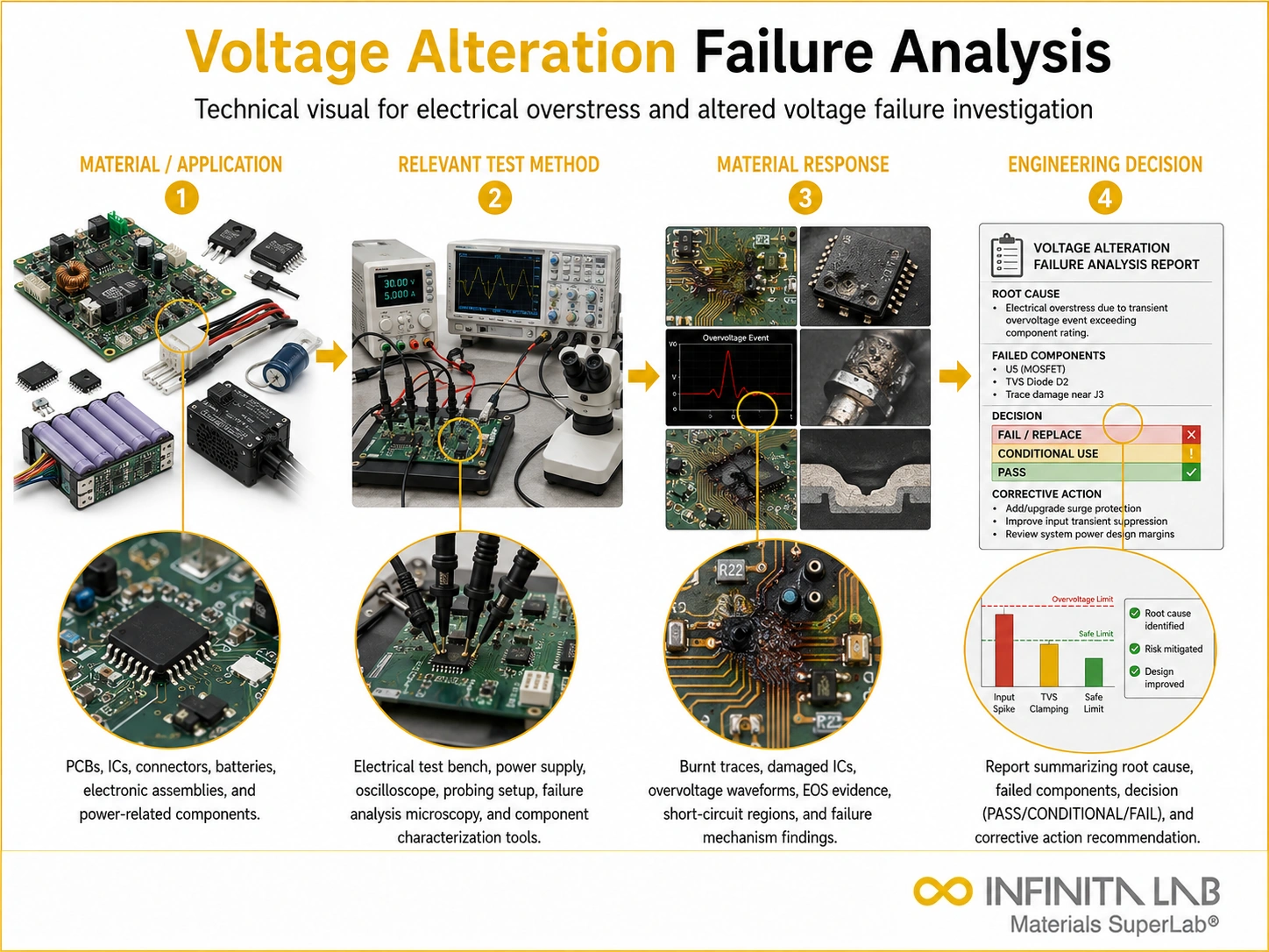
Voltage Alteration Failure Analysis Process
Electrical Characterization and Failure Mode Definition
The failed device is electrically characterized using curve tracer analysis, parametric measurement, and functional testing
1Non-Destructive Inspection
X-ray imaging detects internal package damage, bond wire anomalies, and die attach issues.
2Decapsulation and Die Inspection
The device is opened using chemical, mechanical, or laser decapsulation appropriate to the package type.
3Mechanism Classification and Reporting
Damage morphology, location, electrical signature, and physical evidence are integrated to classify the failure mechanism as ESD
4Voltage Alteration Failure Analysis Technical Specifications
| Parameter | Details |
|---|---|
| Service Type | Investigative failure analysis -voltage-related damage mechanisms in electronic components |
| Failure Mechanisms Covered | ESD (HBM, CDM, MM), EOS (forward/reverse overstress), transient overvoltage, reverse polarity, latch-up, secondary breakdown |
| Electrical Analysis | Curve tracer, parametric measurement, functional testing, leakage characterization |
| Non-Destructive Methods | X-ray (2D and CT), scanning acoustic microscopy (SAM) |
| Physical Analysis | Optical microscopy, SEM, FIB cross-sectioning, TEM specimen preparation |
| Chemical Analysis | EDS elemental mapping for melt, burn, and contamination characterization |


Instrumentation Used for Voltage Alteration Failure Analysis
- Curve tracer and parametric analyzer for electrical failure characterization
- X-ray inspection system and scanning acoustic microscope (SAM)
- Chemical and laser decapsulation systems
- Scanning electron microscope (SEM) with EDS
- Focused ion beam (FIB) system for cross-sectioning and TEM preparation
- Optical microscope with high-magnification imaging
- Transmission electron microscope (TEM) for gate oxide and junction-level analysis where required
Voltage Alteration Failure Analysis Results and Deliverables
- Electrical failure signature before and after physical analysis
- X-ray and SAM images of package-level anomalies
- SEM images of die surface damage -melted metal, burned areas, junction craters, oxide rupture
- EDS elemental maps confirming metal composition of melt or contamination features
- FIB cross-section images showing damage at gate, junction, or metal line level
- Failure mechanism classification -ESD, EOS, transient, reverse bias, or latch-up -with supporting evidence
- Root cause assessment and recommended corrective action
- Full analytical report formatted for engineering, quality, and liability review
Frequently Asked Questions
Voltage Alteration Failure Analysis investigates how abnormal voltage conditions, such as overvoltage, undervoltage, or voltage transients, affect the performance and reliability of electronic components and circuits. It helps identify the root cause of voltage-induced failures.
The analysis can detect failures caused by voltage spikes, brownouts, electrical overstress (EOS), dielectric breakdown, insulation failure, and damage to semiconductor junctions or power management circuits.
The technique is suitable for integrated circuits (ICs), printed circuit boards (PCBs), power supplies, sensors, memory devices, microcontrollers, and other electronic assemblies exposed to abnormal voltage conditions.
Engineers combine electrical measurements with microscopic inspection, thermal analysis, and advanced imaging techniques to locate damaged regions and determine whether the failure resulted from voltage stress or another mechanism.
Why Choose Infinita Lab for Advanced Materials Testing and Characterization?
At the core of this breadth is our network of 2,000+ accredited laboratories across the USA, offering access to over 10,000 testing methods and analytical services. From advanced materials characterization (SEM, TEM, RBS, XPS) to mechanical, chemical, environmental, biological, and standardized ASTM/ISO-compliant testing, we deliver unmatched flexibility, specialization, and scale. You are never limited by geography, facility, or methodology — Infinita Lab connects you to the right expertise and testing solution, every time.

Looking for a Trusted Partner for Accurate and Reliable Testing Services?
Send query us at hello@infinitlab.com or call us at (888) 878-3090 to learn more about our services and how we can support you.


Request a Quote
Submit your material details and receive testing procedures, pricing, and turnaround time within 24 hours.
 Quick Turnaround and Hasslefree process
 Confidentiality Guarantee
 Free, No-obligation Consultation
 100% Customer Satisfaction
