


Isolating Defective Electronic Devices Testing Services
The dense arrangement of components on circuit boards makes failure analysis of sophisticated systems difficult. To narrow down the field of candidates and isolate the problematic component, a plan is essential. Schematics and board layouts can be used to locate trouble spots. To determine the cause of the failure, the circuit must be changed, and electrical tests must be run. Failure analysis can start as soon as the problematic component has been located. For an exam to be successful, careful planning and iterative testing are necessary.
TRUSTED BY


Get compliant results — request your isolating defective electronic devices testing quote
- Overview
- Scope, Applications, and Benefits
- Test Process
- Specifications
- Instrumentation
- Results and Deliverables
What Is Isolating Defective Electronic Devices?
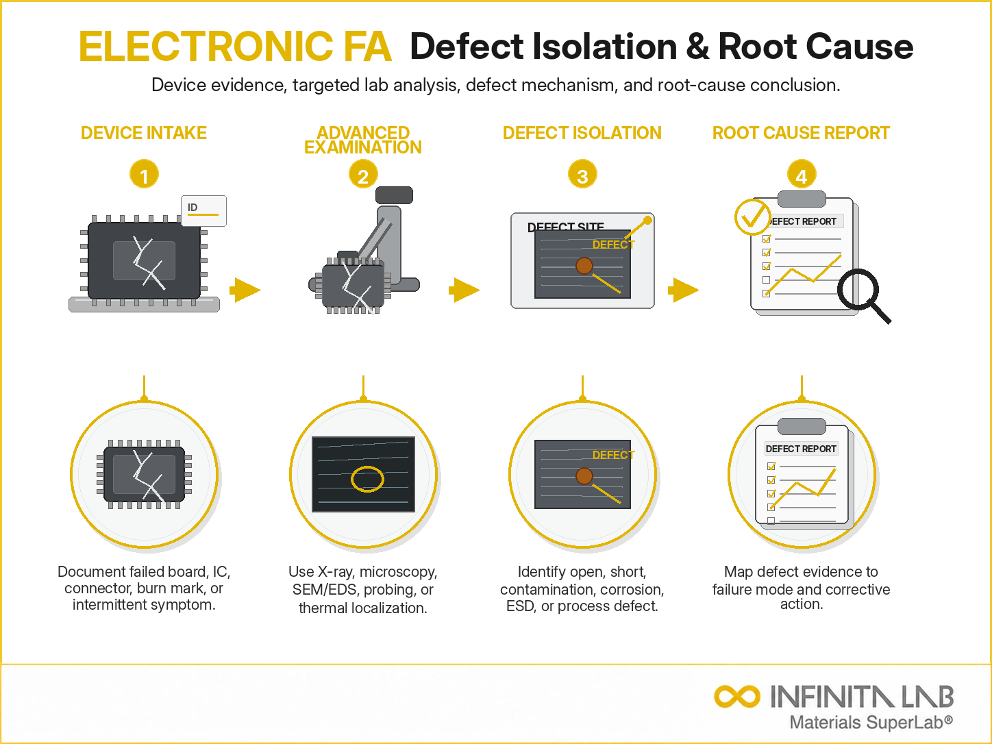
Fault isolation is the process of narrowing down the exact location of a defect within an electronic assembly, printed circuit board (PCB), or integrated circuit (IC) so that root cause failure analysis can proceed efficiently. As component density on modern boards and packages increases, the number of candidate failure sites grows accordingly, making a structured, iterative approach essential. Fault isolation combines schematic and layout review, electrical testing, and physical/optical inspection techniques to progressively eliminate known-good circuit sections and converge on the specific component, solder joint, die location, or interconnect responsible for an observed failure.
Fault isolation is typically the first stage of a broader failure analysis workflow. Once a suspect site has been localized, downstream techniques — decapsulation, cross-sectioning, SEM/EDS, X-ray inspection, or electrical curve tracing — can be applied to confirm and characterize the failure mechanism. Without effective isolation, destructive analysis techniques risk being applied to the wrong location, wasting time and destroying evidence needed for root cause determination.

Applications and Benefits of Isolating Defective Electronic Devices Testing
Scope
Fault isolation applies to electronic assemblies and devices at multiple levels of the packaging hierarchy:
- Board-level assemblies — populated PCBs, multi-chip modules, and hybrid assemblies exhibiting intermittent or hard failures, opens, shorts, or out-of-specification electrical behavior
- Component-level devices — discrete components, connectors, and passive devices suspected of internal defects
- Integrated circuits and packages — silicon die, wire bonds, flip-chip interconnects, and package-level defects including delamination, cracking, and electrical overstress damage
- Interconnect and via structures — solder joints, through-hole plating, BGA balls, and buried vias where marginal connections cause intermittent faults
Applications
- Field return analysis — determining why a returned unit failed in service, to support corrective action and warranty decisions
- New product introduction debug — isolating design or process-related defects during bring-up of new boards or packages
- Manufacturing yield improvement — identifying systematic failure sites across a production lot to guide process corrections
- Reliability and qualification testing support — localizing failures that occur during environmental stress screening, burn-in, or accelerated life testing
- Counterfeit and supply chain investigations — isolating anomalies that indicate non-conforming or substituted components
Benefits
- Preserves evidence for root cause analysis — narrowing the search area before applying destructive techniques prevents loss of failure evidence
- Reduces analysis time and cost — a structured, iterative isolation process avoids unnecessary testing of known-good circuit areas
- Supports corrective and preventive action — precise localization of the failure site is necessary to identify the true failure mechanism and prevent recurrence
- Applicable across the packaging hierarchy — the same general methodology scales from board-level assemblies down to individual die features
Our Testing Procedure
Review Documentation
Examine schematics, layouts, drawings, and test data to identify possible failure locations.
1Perform Non-Intrusive Testing
Use electrical measurements and visual inspection to detect opens, shorts, damage, or abnormal behaviour.
2Localise the Fault
Apply thermal imaging, emission microscopy, X-ray, or other isolation techniques to pinpoint the defective area.
3Confirm and Document
Isolate and retest the circuit, then document the fault location for detailed failure analysis.
4Test parameters and requirements
| Parameter | Details |
|---|---|
| Applicable Devices | PCBs, multi-chip modules, discrete components, ICs, packages, interconnects |
| Common Techniques | Curve tracing, thermal imaging, liquid crystal hot-spot detection, photon emission microscopy, X-ray inspection, time-domain reflectometry (TDR), optical microscopy |
| Typical Failure Modes Investigated | Opens, shorts, intermittent connections, electrical overstress, latent defects, corrosion |
| Related Follow-On Analysis | Decapsulation, cross-sectioning, SEM/EDS, die-level electrical analysis |
| Output | Localized failure site with supporting electrical and imaging data |


- Curve tracer or parametric analyzer for component-level electrical characterization
- Digital multimeter and LCR meter for continuity, resistance, and impedance measurements
- Thermal imaging camera for hot-spot detection under bias
- Liquid crystal hot-spot detection setup for localized thermal anomalies on powered devices
- Photon emission microscope for detecting light emission associated with electrical faults
- X-ray inspection system for internal package and interconnect visualization
- Time-domain reflectometer (TDR) for locating opens and impedance discontinuities along signal paths
- Stereo and digital optical microscopes for visual inspection at varying magnification
Equipment and Instrumentation Used for Testing
What You Receive: Test Report, Data, and Certification
- Fault isolation report — documentation of the review process, techniques applied, and results at each stage of the isolation process
- Localized failure site identification — the specific component, interconnect, or die-level feature identified as the probable failure location
- Supporting electrical data — curve traces, resistance/continuity measurements, and any anomalous readings recorded during testing
- Imaging documentation — thermal, optical, X-ray, or emission microscopy images supporting the localization findings
- Recommendations for further analysis — guidance on appropriate destructive or physical analysis techniques to confirm root cause at the isolated site
Isolating Defective Electronic Devices FAQs
Accurate fault isolation reduces repair time, avoids unnecessary component replacement and prevents recurring failures. It also supports product reliability, manufacturing improvement and root-cause analysis.
The process usually begins by reviewing failure symptoms, operating history, schematics and test data. A visual inspection is then performed to identify burns, corrosion, cracked parts or loose connections.
Signal tracing follows an electrical signal through different stages of a circuit. The point where the signal becomes missing, distorted or incorrect helps identify the defective section.
X-ray imaging, thermal imaging and scanning acoustic microscopy can reveal hidden defects without damaging the device. These methods may detect short circuits, hot spots, voids, cracks and delamination.
Yes. Intermittent faults may be investigated using continuous monitoring, vibration, temperature cycling or electrical stressing. Data logging helps capture the conditions under which the failure appears.
Why Choose Infinita Lab for Isolating Defective Electronic Devices Testing?
At the core of this breadth is our network of 2,000+ accredited laboratories across the USA, offering access to over 10,000 testing methods and analytical services. From advanced materials characterization (SEM, TEM, RBS, XPS) to mechanical, chemical, environmental, biological, and standardized ASTM/ISO-compliant testing, we deliver unmatched flexibility, specialization, and scale. You are never limited by geography, facility, or methodology — Infinita Lab connects you to the right expertise and testing solution, every time.

Looking for an Accredited Partner for Isolating Defective Electronic Devices Testing?
Send query us at hello@infinitalab.com or call us at (888) 878-3090 to learn more about our services and how we can support you.



Request a Quote
Submit your material details and receive testing procedures, pricing, and turnaround time within 24 hours.
 Quick Turnaround and Hasslefree process
 Confidentiality Guarantee
 Free, No-obligation Consultation
 100% Customer Satisfaction
