


Electronic Component Failure Analysis
The process of conducting an electronic component failure analysis entails locating and isolating malfunctioning parts of an electronic system. Understanding the underlying reasons for failures and putting the right corrective measures in place depend on this process.
TRUSTED BY


Electronic Component Failure Analysis
- Overview
- Scope, Applications, and Benefits
- Test Process
- Specifications
- Instrumentation
- Results and Deliverables
Electronic Component Failure Analysis Overview
Electronic component failure analysis is the process of determining why a component stopped working, worked intermittently, or degraded in performance -and tracing that failure back to its root cause. The component could be a transistor, an integrated circuit, a capacitor, a resistor, a connector, a diode, or any discrete or packaged electronic device. What failed at the electrical level is usually apparent from testing. What caused it to fail, and whether the cause was design, manufacturing, handling, application, or environment, requires a structured physical investigation.
The analysis follows a defined sequence: start with electrical characterization to understand what the device is doing wrong, work non-destructively first to preserve options, then progress to physical and chemical analysis of the die, package, interconnects, and materials to identify where the damage is and what mechanism produced it. Common failure mechanisms include electrostatic discharge (ESD) damage, electrical overstress (EOS), electromigration in metal interconnects, corrosion and ionic contamination, dielectric breakdown, bond wire failures, package delamination, and solder joint fatigue. Each mechanism leaves characteristic physical evidence that an experienced analyst can identify.
At Infinita Lab, we coordinate electronic component failure analysis through our network of accredited labs equipped with the full range of electrical and physical analysis tools. Whether the driver is a field return investigation, a reliability qualification failure, a supplier dispute, or a product safety concern, we connect clients to the right analytical expertise and help build a technically defensible case from symptom to root cause.

Electronic Component Failure Analysis Scope, Applications, and Benefits
Scope
Electronic component failure analysis covers active and passive components, including integrated circuits, transistors, MOSFETs, diodes, capacitors, resistors, inductors, connectors, and sensors in any package format -through-hole, surface mount, BGA, QFN, flip-chip, bare die, and module assemblies. The analysis workflow spans electrical characterization to define and reproduce the failure signature, non-destructive inspection including X-ray and scanning acoustic microscopy to locate internal damage, physical decapsulation and die access to expose internal structures, surface and die-level imaging by optical microscopy and SEM, elemental and materials characterization by EDS, XRF, and FTIR, and focused ion beam (FIB) cross-sectioning for sub-micron feature analysis. Failure mechanisms covered include ESD, EOS, electromigration, corrosion, dielectric breakdown, bond wire degradation, package cracking, delamination, and manufacturing-related defects. Analysis can be scoped to a single component or extended to a lot or fleet investigation.
Applications
- Field return and customer complaint investigation for failed electronic components
- ESD and EOS damage identification and source tracing
- Reliability qualification failure investigation during HTOL, HAST, or temperature cycling
- Electromigration and time-dependent dielectric breakdown (TDDB) failure characterization
- Bond wire and interconnect failure analysis -opens, corrosion, Kirkendall voiding
- Package-level failures -delamination, moisture-induced cracking, lid seal integrity
- Counterfeit component detection and authentication
- Supplier qualification and incoming lot rejection investigation
- Product liability and safety investigation requiring documented root cause findings
- Failure mode and effects analysis (FMEA) supports with physical evidence of known failure modes
Benefits
- Structured analysis workflow prevents evidence destruction and maximizes information recovered from each sample
- Non-destructive inspection first means destructive steps are targeted and purposeful rather than exploratory
- Covers the full failure mechanism library -ESD, EOS, electromigration, corrosion, dielectric breakdown, and more
- Physical evidence documented with images, spectra, and measurements that support engineering and legal review
- Distinguishes between manufacturing defects, application damage, handling damage, and design weaknesses
- FIB and TEM capability enables sub-micron defect analysis down to the transistor and interconnect level
- Applicable across all component types, package formats, and technology nodes
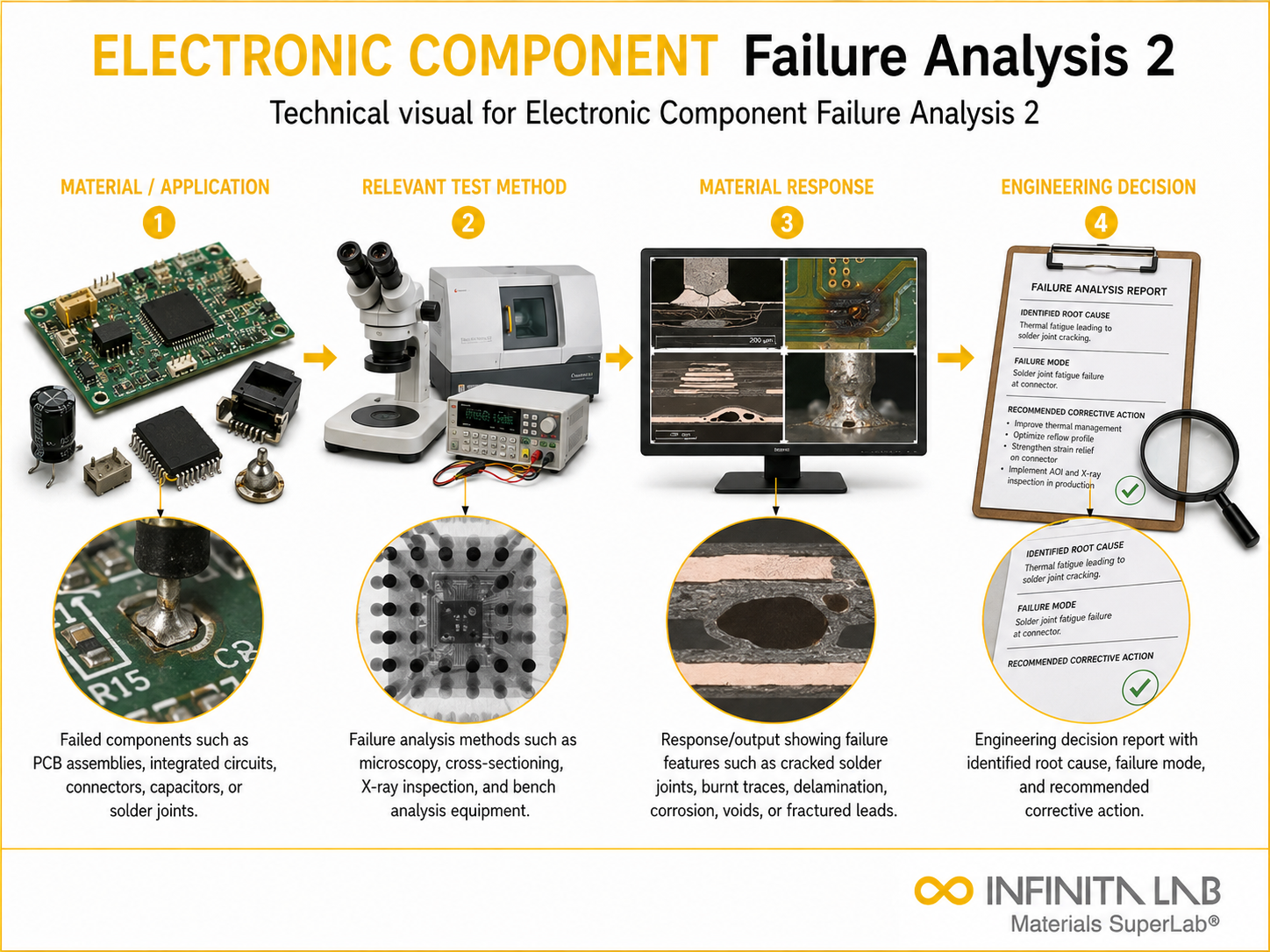
Electronic Component Failure Analysis Process
Electrical Characterization and Failure Verification
The failed component is electrically tested to document and reproduce the failure signature -leakage currents, parametric shifts, opens, shorts, or functional failures.
1Non-Destructive Physical Inspection
X-ray imaging is performed to inspect internal wire bonds, die attach, solder connections, and package integrity without opening the device.
2Decapsulation and Die-Level Analysis
he component is opened using mechanical, chemical, or laser decapsulation as appropriate for the package type and failure location.
3Root Cause Determination and Reporting
All electrical, physical, and chemical findings are correlated to identify the failure mechanism and its probable origin.
4Electronic Component Failure Analysis Technical Specifications
| Parameter | Details |
|---|---|
| Service Type | Investigative analytical service -technique sequence driven by failure mode and component type |
| Component Types | ICs, transistors, diodes, capacitors, resistors, connectors, sensors -all package formats |
| Electrical Analysis | Curve tracer, parametric measurement, functional testing, leakage and resistance characterization |
| Non-Destructive Methods | X-ray (2D and CT), scanning acoustic microscopy (SAM) |
| Physical Analysis | Optical microscopy, SEM, FIB cross-sectioning, TEM specimen preparation |
| Chemical and Elemental Analysis | EDS, XRF, FTIR, and Auger electron spectroscopy (AES), where applicable |


Instrumentation Used for Electronic Component Failure Analysis
- Curve tracer and parametric analyzer for electrical failure characterization
- X-ray inspection system (2D radiography and computed tomography)
- Scanning acoustic microscope (SAM) for package-level delamination and void detection
- Chemical decapsulation station with fuming acid and jet etch capability
- Laser decapsulation system for precision package opening
- Scanning electron microscope (SEM) with energy dispersive X-ray spectroscopy (EDS)
- Focused ion beam (FIB) system for cross-sectioning and TEM specimen preparation
- Optical microscope with high-magnification imaging and measurement capability
- Transmission electron microscope (TEM) for atomic-scale defect characterization
Electronic Component Failure Analysis Results and Deliverables
- Electrical failure signature documentation with measured parameters before and after analysis
- X-ray and SAM images showing internal package structure and any detected anomalies
- The surface and bond wire SEM images with identified damage features
- EDS elemental maps and spectra for corrosion products, deposits, or contamination
- FIB cross-section images showing subsurface defects at the interconnect, gate, or dielectric level
- Failure mechanism classification with physical evidence supporting the determination
- Root cause assessment, identifying whether the origin is manufacturing, handling, application, or environment
- Full analytical report with all data, images, and conclusions formatted for engineering, quality, or legal review
Frequently Asked Questions
Details such as circuit conditions, operating voltage, failure history, environmental exposure, and PCB layout significantly improve the ability to isolate the true root cause efficiently.
In many cases, yes. Even after partial failure, electrical characterization can reveal abnormal leakage, open/short conditions, or degraded performance before destructive analysis is performed.
It identifies the root cause of failure in components such as ICs, resistors, capacitors, and sensors. The analysis links electrical symptoms to physical or material-level damage mechanisms.
Yes. By correlating electrical behavior with physical inspection, analysts can distinguish between design flaws, manufacturing defects, and field-related stresses such as overload or thermal cycling.
Typical methods include electrical testing, optical microscopy, X-ray imaging, decapsulation, SEM/EDS analysis, and thermal or emission-based diagnostics depending on the failure type.
Why Choose Infinita Lab for Advanced Materials Testing and Characterization?
At the core of this breadth is our network of 2,000+ accredited laboratories across the USA, offering access to over 10,000 testing methods and analytical services. From advanced materials characterization (SEM, TEM, RBS, XPS) to mechanical, chemical, environmental, biological, and standardized ASTM/ISO-compliant testing, we deliver unmatched flexibility, specialization, and scale. You are never limited by geography, facility, or methodology — Infinita Lab connects you to the right expertise and testing solution, every time.

Looking for a Trusted Partner for Accurate and Reliable Testing Services?
Send query us at hello@infinitlab.com or call us at (888) 878-3090 to learn more about our services and how we can support you.


Request a Quote
Submit your material details and receive testing procedures, pricing, and turnaround time within 24 hours.
 Quick Turnaround and Hasslefree process
 Confidentiality Guarantee
 Free, No-obligation Consultation
 100% Customer Satisfaction
