


Emission Microscopy (EMMI) Analysis
Electronic failure analysis is crucial to ensuring the consistent performance of your ground-breaking circuit board technology. Due to the intricacy of circuit boards and their nanoscale components, DIY or in-house troubleshooting techniques are inadequate. Reliable failure analysis gives you a number of ways to find problems like semiconductors, integrated circuits, or parts that are rated incorrectly. Some methods that can be used to find broken connections, internal faults, and microscopic issues are dry deprocessing, scanning acoustic microscopy (SAM), and emission microscopy. By enlisting the help of Insight Analytical Laboratories, Inc., you can gain insights and learn failure avoidance techniques.
TRUSTED BY


Precision-driven testing for dimensional accuracy and compliance
- Overview
- Scope, Applications, and Benefits
- Test Process
- Specifications
- Instrumentation
- Results and Deliverables
Emission Microscopy Failure Analysis Overview
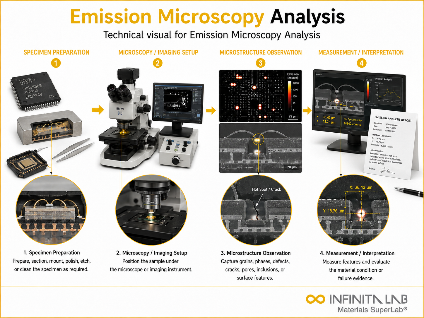
Emission microscopy (EMMI) is a failure analysis technique used to locate defects in semiconductor devices and integrated circuits by detecting the faint light emitted from active failure sites. When a defect such as a leakage path, junction breakdown, or gate oxide failure is present, the abnormal current flow generates a small amount of photon emission. A highly sensitive detector captures this emission and overlays it onto an optical image of the device, pinpointing the exact physical location of the fault.
The technique is non-destructive and is typically one of the first fault-isolation steps performed when a failing device needs to be localized before any physical deprocessing begins. Because modern ICs contain millions of features at nanoscale dimensions, blindly cross-sectioning or deprocessing a device without first knowing where the fault is located is impractical. Emission microscopy provides that location, dramatically narrowing the area that subsequent physical analysis needs to examine.
Emission microscopy is widely used alongside other fault-isolation methods such as thermal (lock-in thermography) and laser-based techniques (OBIRCH, LIVA), and is followed by physical analysis methods like FIB cross-sectioning and SEM imaging to confirm the root cause at the located site. It is a core capability in semiconductor and IC failure analysis.

Emission Microscopy Failure Analysis Scope, Applications, and Benefits
Scope
Emission microscopy covers the detection and localization of photon-emitting defects in semiconductor devices, integrated circuits, and related electronic components. The technique detects light emission from sites of abnormal electrical activity while the device is electrically biased, and maps that emission to a physical location on the device.
Key aspects of the technique include:
- Photon emission detection – captures faint light emitted from active failure sites using highly sensitive detectors (such as cooled CCD, InGaAs, or photomultiplier-based systems) operating from the visible into the near-infrared range
- Front-side and backside analysis – emission can be detected from the front (circuit) side or, increasingly for flip-chip and multilayer devices, from the backside through the silicon using near-infrared-sensitive detectors
- Biased-device operation – the device is electrically biased into the failing condition during analysis so that the defect actively emits; static and dynamic bias conditions can be applied depending on the failure
- Defect types detected – junction leakage, gate oxide breakdown, latch-up, ESD damage, hot-carrier effects, dielectric defects, and other sites of abnormal current flow
- Image overlay – the captured emission is superimposed on a reference optical image of the device to precisely identify the location of the emission site
- Complementary techniques – frequently combined with thermal emission (lock-in thermography), OBIRCH, and laser stimulation methods for comprehensive fault isolation
Applications
- Semiconductor device fault isolation – locating leakage, short, and breakdown sites in transistors, diodes, and IC structures as the first step before physical failure analysis
- Integrated circuit failure analysis – pinpointing defects in complex ICs where the failing area must be located among millions of features before deprocessing
- Gate oxide and dielectric defect localization – detecting emission from gate oxide breakdown and dielectric defects that cause leakage or device failure
- ESD and EOS damage localization – finding the physical site of electrostatic discharge or electrical overstress damage within a device
- Latch-up investigation – locating latch-up sites in CMOS devices where parasitic structures cause abnormal current flow
- Product and reliability failure analysis – investigating devices that failed during qualification, burn-in, or field use to localize the defect and support root cause determination
- Process and yield improvement – identifying recurring defect locations across failing devices to feed back into process and design improvements
Benefits
- Non-destructive fault localization – emission microscopy locates the defect without altering or damaging the device, preserving it for subsequent physical analysis at the identified site
- Dramatically narrows the analysis area – by pinpointing the emission site, the technique reduces the area that costly and time-consuming physical deprocessing must examine, from the whole die down to a specific feature
- Detects a wide range of defect types – because many different failure mechanisms produce photon emission, EMMI is broadly applicable across leakage, breakdown, ESD, and dielectric failures
- Backside capability for modern packages – near-infrared detection through the silicon enables analysis of flip-chip and multilayer devices where the front side is inaccessible
- Complements other fault-isolation methods – used together with thermal and laser techniques, emission microscopy contributes to a comprehensive fault-isolation workflow that maximizes the chance of locating elusive defects
Emission Microscopy Failure Analysis Test Process
Prepare the Device
Mount and connect the device, prepare the package if needed, and capture a reference image.
1Apply Electrical Bias
Operate the device under the failing condition to activate the defect site.
2Detect Emissions
Capture photon emissions with a sensitive detector in a dark enclosure.
3Locate and Report
Overlay the emission image on the reference image to identify and document the defect location.
4Emission Microscopy Failure Analysis Technical Specifications
| Parameter | Details |
|---|---|
| Detector Types | Cooled CCD, InGaAs, or photomultiplier-based (visible to near-IR) |
| Analysis Side | Front-side and backside (through-silicon, near-IR) |
| Bias Conditions | Static or dynamic electrical bias into the failing state |
| Defects Detected | Junction leakage, gate oxide breakdown, latch-up, ESD/EOS, dielectric defects, hot carriers |
| Output | Emission site location overlaid on optical device image |
| Device Types | Semiconductors, ICs, transistors, diodes, discrete devices |
| Nature | Non-destructive fault isolation |
| Complementary Methods | Lock-in thermography, OBIRCH, LIVA, FIB/SEM (follow-up) |


Instrumentation Used for Emission Microscopy Failure Analysis
- Emission microscope system with high-sensitivity photon detector (CCD/InGaAs)
- Light-tight enclosure for low-light emission detection
- Device bias and parametric source/measure equipment
- Backside sample preparation tools (thinning and polishing) for through-silicon analysis
- Optical microscope for reference imaging
- Image processing and overlay software
Emission Microscopy Failure Analysis Results and Deliverables
- Fault isolation report – documented emission site location overlaid on the optical image of the device, identifying where the defect is physically located
- Emission images – captured emission overlaid on the device layout, showing the active site(s) detected under bias
- Bias condition records – the electrical bias conditions under which emission was detected, supporting interpretation of the failure mechanism
- Site localization detail – physical coordinates or layout reference for the emission site to guide subsequent physical analysis
- Recommendations for follow-up – suggested next steps (e.g., FIB cross-section, SEM, deprocessing) at the located site to confirm root cause
- Sample records – device identification, package condition, and any preparation (e.g., backside thinning) performed
Frequently Asked Questions
The device is electrically powered while a highly sensitive camera records photon emissions from the semiconductor surface. Emission hotspots are then overlaid on a device image or circuit layout.
Light may be generated by accelerated charge carriers, junction breakdown, leakage current or transistor switching. Abnormal emissions can indicate electrically overstressed or defective regions.
It can help locate junction leakage, gate-oxide damage, latch-up, ESD damage, defective transistors and certain short circuits. Detection depends on whether the failure produces measurable light.
Photon emission microscopy, or PEM, is another name commonly used for emission microscopy. It employs sensitive optical detectors to capture extremely weak light from operating semiconductor devices.
Frontside analysis observes emissions from the circuit side of the die. It may require removal of moulding compounds, lids or protective coatings that block optical access.
Why Choose Infinita Lab for Advanced Materials Testing and Characterization?
At the core of this breadth is our network of 2,000+ accredited laboratories across the USA, offering access to over 10,000 testing methods and analytical services. From advanced materials characterization (SEM, TEM, RBS, XPS) to mechanical, chemical, environmental, biological, and standardized ASTM/ISO-compliant testing, we deliver unmatched flexibility, specialization, and scale. You are never limited by geography, facility, or methodology — Infinita Lab connects you to the right expertise and testing solution, every time.

Looking for a Trusted Partner for Accurate and Reliable Testing Services?
Send query us at hello@infinitlab.com or call us at (888) 878-3090 to learn more about our services and how we can support you.



Request a Quote
Submit your material details and receive testing procedures, pricing, and turnaround time within 24 hours.
 Quick Turnaround and Hasslefree process
 Confidentiality Guarantee
 Free, No-obligation Consultation
 100% Customer Satisfaction
