


Memory Device Failure Analysis Testing Services
This topic explores the crucial role of memory testing in failure analysis services. It highlights the process of identifying and analyzing memory failures in electronic systems, including the detection of errors, faults, and defects. Memory testing plays a vital role in ensuring reliable and efficient performance of digital devices.
TRUSTED BY


Get compliant results — request your memory device failure analysis testing quote
- Overview
- Scope, Applications, and Benefits
- Test Process
- Specifications
- Instrumentation
- Results and Deliverables
What Is Memory Device Failure Analysis?
Memory devices are among the most structurally complex and density-sensitive components in modern electronics. A single NAND flash die can contain hundreds of billions of cells stacked in three dimensions, each storing charge in a tunnel oxide layer only a few nanometers thick. At these dimensions, failures can originate from defects invisible to optical inspection – a trapped charge, a voided via, a grain boundary in a metal interconnect, or a sub-nanometer oxide thinning from a process excursion.
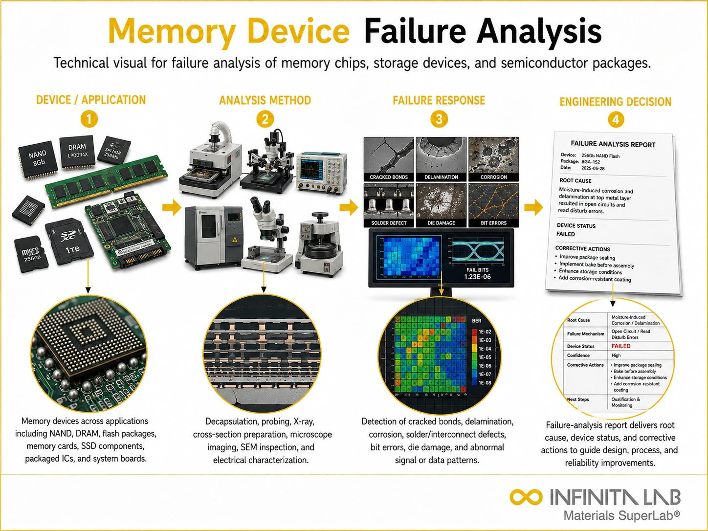
Memory device failure analysis maps the invisible failure to a physical and chemical root cause. The process begins with electrical characterization to reproduce and classify the failure mode – single-bit errors, multi-bit upsets, retention loss, endurance degradation, or catastrophic open/short faults. That electrical signature then guides the physical analysis: which die, block, cell array, and layer to deprocess. Targeted techniques – focused ion beam (FIB) cross-sectioning, transmission electron microscopy (TEM), energy-dispersive X-ray spectroscopy (EDS), and secondary ion mass spectrometry (SIMS) – then resolve the defect at atomic or near-atomic resolution.
The result is a root cause conclusion traceable to a specific material, process step, design margin, or use condition – actionable information that feeds directly into corrective action, process optimization, or warranty claim decisions.

Applications and Benefits of Memory Device Failure Analysis Testing
Scope
Memory device failure analysis covers the full analytical workflow from failed device intake to root cause report -electrical fault isolation, non-destructive inspection, package decapsulation, die-level deprocessing, electron microscopy, and elemental analysis.
Applicable memory types: DRAM (DDR3/4/5, LPDDR4/5), NAND flash (2D and 3D, SLC/MLC/TLC/QLC), NOR flash, SRAM, EEPROM, MRAM, PCRAM, ReRAM, and HBM/HMC devices.
The scope does not cover device re-programming, data recovery, or firmware-level diagnostics. Focus is on physical and electrical root cause determination at the component and materials level.
Applications
- Semiconductor qualification & reliability -JEDEC-standard stress testing (HTOL, HAST, THB, ESD) followed by failure analysis on stressed devices to verify failure modes and confirm margin against spec
- Field return investigation -systematic analysis of customer-returned memory modules and embedded memory components to determine whether failure originated from manufacturing defect, ESD damage, overstress, or end-use condition
- Process development & yield improvement -identification of process-induced defects during technology node development or process transfer, with defect density mapping and root cause attribution to specific process steps
- Supplier qualification -independent third-party analysis of memory components from new or alternate suppliers to verify conformance to specification and screen for latent defects before design-in
- FMEA support -physical evidence for FMEA inputs in automotive, medical, and aerospace memory applications where safety-critical reliability documentation is required
Benefits
- Electrical-to-physical traceability -connects the electrical fault signature (bit, address, fail pattern) to a specific physical defect location; without this connection, corrective action targets the wrong variable, and the failure recurs
- Sub-nanometer defect resolution -TEM and STEM imaging resolve defects at the atomic scale -a 2 nm oxide pinhole, monolayer contamination at a gate interface, a single-void interconnect; no other analytical method reaches this resolution on real device structures
- Multi-technique root cause confidence -combining FIB, TEM, EDS, and SIMS on the same defect site produces convergent evidence from independent modalities -the standard of proof for actionable corrective action
- Accelerated corrective action cycle -precise root cause identification shortens the corrective action loop from months to weeks; every unanalyzed process excursion is another yield loss cycle
Our Testing Procedure
Electrical Characterization and Non-Destructive Inspection
The failed device is electrically tested to reproduce and classify the failure.
1Decapsulation and Die Access
The package encapsulant is using wet chemical or plasma-based methods
2Defect Localization
Fault isolation techniques, including emission microscopy, laser voltage probing, and light-induced voltage alteration, are applied
3Physical Analysis and Root Cause Determination
Focused ion beam cross-sectioning is performed at the identified defect site.
4Test parameters and requirements
| Parameter | Details |
|---|---|
| Memory Types Supported | DRAM, LPDDR, SRAM, NAND Flash, NOR Flash, eMMC, UFS |
| Package Types | BGA, CSP, QFN, DIP, SOP, bare die, memory modules |
| Inspection Methods | X-ray, scanning acoustic microscopy (SAM), optical microscopy, SEM |
| Physical Analysis Techniques | Decapsulation (chemical, mechanical, laser), FIB cross-section, polishing |
| Analytical Techniques | EDS, TEM, EELS, SIMS, AFM |
| Electrical Analysis | Bit error mapping, retention testing, parametric characterization |
| Report Output | Root cause analysis report with images, data, and corrective input |


- Focused ion beam (FIB) system -Ga+ and Xe plasma beam platforms
- Transmission electron microscope (TEM/STEM) with EDS and EELS detectors
- Scanning electron microscope (SEM) with EDS
- Emission microscope (EMMI) and laser-based fault isolation tools (LVP, LIVA)
- Scanning acoustic microscope (C-SAM)
- X-ray inspection system (2D and computed tomography)
- Wet chemical and plasma decapsulation stations
- Secondary ion mass spectrometer (SIMS)
- X-ray photoelectron spectrometer (XPS)
- Automated memory tester and parametric measurement unit (PMU)
Equipment and Instrumentation Used for Testing
What You Receive: Test Report, Data, and Certification
- Identified failure mechanism with physical and electrical evidence
- FIB cross-section images showing defect location and morphology
- SEM and optical micrographs of the die surface and package internals
- Bit error maps and electrical characterization data
- Elemental composition data from EDS, EELS, or SIMS, where applicable
- Root cause summary with failure origin classification
- Recommendations for corrective action or process investigation
- Detailed technical report formatted for engineering review
Memory Device Failure Analysis FAQs
Yes. A comprehensive failure analysis combines electrical characterization, non-destructive imaging (such as X-ray or scanning acoustic microscopy), decapsulation, and microscopic inspection to identify the failure mechanism. This helps differentiate process-related defects from EOS, ESD, mechanical damage, contamination, or wear-out mechanisms.
In many cases, yes. If the failure has not permanently damaged the memory cells, data recovery may be possible before destructive analysis begins. Recovery methods depend on the device type (NAND Flash, NOR Flash, EEPROM, DRAM, etc.), package condition, and the nature of the failure. If data preservation is critical, this should be communicated before testing.
Intermittent failures often require a combination of electrical testing, thermal or environmental stress screening, emission microscopy (EMMI), photon emission analysis, thermal imaging, focused ion beam (FIB) cross-sectioning, SEM/EDS analysis, and circuit editing. Selecting the appropriate techniques depends on whether the issue is related to timing, leakage current, metallization defects, package integrity, or die-level damage.
Yes. Engineers evaluate wear indicators such as program/erase cycle degradation, oxide breakdown, electromigration, solder fatigue, corrosion, moisture ingress, and thermal damage. By correlating physical evidence with device history and operating conditions, it is often possible to distinguish premature field failures from expected wear-out mechanisms.
Providing the device part number, failure symptoms, operating conditions, test results, and known-good comparison samples helps engineers perform a more accurate and efficient root cause investigation.
Why Choose Infinita Lab for Memory Device Failure Analysis Testing?
At the core of this breadth is our network of 2,000+ accredited laboratories across the USA, offering access to over 10,000 testing methods and analytical services. From advanced materials characterization (SEM, TEM, RBS, XPS) to mechanical, chemical, environmental, biological, and standardized ASTM/ISO-compliant testing, we deliver unmatched flexibility, specialization, and scale. You are never limited by geography, facility, or methodology — Infinita Lab connects you to the right expertise and testing solution, every time.

Looking for an Accredited Partner for Memory Device Failure Analysis Testing?
Send query us at hello@infinitalab.com or call us at (888) 878-3090 to learn more about our services and how we can support you.



Request a Quote
Submit your material details and receive testing procedures, pricing, and turnaround time within 24 hours.
 Quick Turnaround and Hasslefree process
 Confidentiality Guarantee
 Free, No-obligation Consultation
 100% Customer Satisfaction
