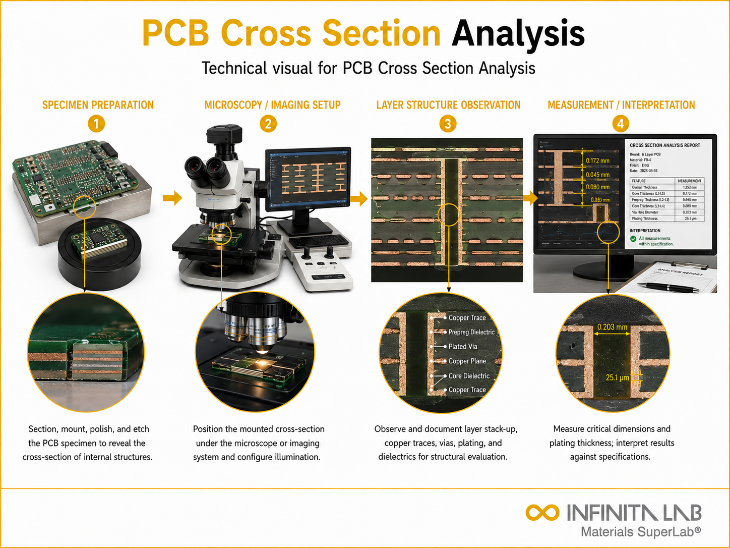


What Is PCB Cross Section Analysis?
PCB cross-section analysis is the primary destructive technique for evaluating the internal structural quality of a printed circuit board. It involves mounting a section of the board in epoxy resin, cutting through the region of interest, and progressively grinding and polishing the cross-section to expose the target feature plane a plated through-hole, a via, a solder joint, a blind or buried via, or a specific layer interface. The exposed cross-section is then examined under optical and electron microscopy to measure dimensions, evaluate material quality, and identify defects.
What cross-sectioning reveals cannot be seen by any surface or non-destructive inspection method. Copper plating thickness in through-holes and vias, hole wall quality including etch uniformity and smear, barrel crack presence and morphology, wicking into laminate, innerlayer registration and copper annular ring width, solder joint microstructure and intermetallic compound layers, void content in via fill materials, and laminate delamination at drill-induced interfaces are all only accessible through a well-prepared cross-section. These features directly determine whether a PCB will survive its intended service life and pass reliability testing.
PCB cross-section analysis is performed to IPC-TM-650 Method 2.1.1 for microsection preparation, and acceptance criteria for the measured features are defined in IPC-A-600 (bare board acceptability), IPC-6012 (qualification and performance specification for rigid boards), and J-STD-001 (soldering requirements for electrical assemblies). Results from cross-section analysis directly support incoming inspection, process troubleshooting, reliability investigation, and IPC conformance assessments.

Applications and Benefits of PCB Cross Section Analysis Testing
Scope
PCB cross-section analysis covers bare boards, assembled boards, and individual components across all board constructions including single-sided, double-sided, and multilayer rigid boards, as well as rigid-flex and high-density interconnect (HDI) boards with blind and buried vias. Features evaluated include through-hole plating thickness and distribution, hole wall quality, barrel and knee cracks, innerlayer connection quality, via fill void content, solder joint microstructure and intermetallic compound (IMC) thickness, pad and land geometry, laminate ply and fiber condition, and layer-to-layer registration. Preparation follows IPC-TM-650 Method 2.1.1. Acceptance criteria are applied per IPC-A-600, IPC-6012, IPC-6013, J-STD-001, or customer-specific workmanship standards as applicable.
Applications
- Incoming PCB inspection plating thickness and hole wall quality verification on new board lots
- IPC Class 2 and Class 3 conformance assessment for bare boards and assemblies
- Failure analysis identifying the root cause of opens, intermittents, and reliability failures
- Barrel crack investigation following thermal cycling or lead-free reflow stress
- Blind via and buried via fill quality assessment for HDI boards
- Solder joint IMC characterization after reflow thin, continuous IMC versus excessive or voided joints
- Supplier process qualification and audit evaluating fabricator plating process consistency
- Thermal cycling test coupon evaluation for reliability qualification programs
Benefits
- Only method that directly reveals copper plating distribution, hole wall integrity, and innerlayer connections
- Results referenced to IPC-A-600 and IPC-6012 acceptance criteria provide objective pass/fail determination
- Identifies process-related defects over-etch, under-plate, smear, delamination that other methods miss
- Applicable to through-holes, vias, solder joints, and laminate features all in the same section
- High-magnification optical and SEM imaging documents defect morphology for root cause analysis
- Supports both incoming inspection programs and failure investigation with the same analytical technique
- Results applicable to IPC Class 1, 2, and 3 conformance assessments
PCB Cross-Section Analysis Process
Sample Selection and Marking
The specific features to be cross-sectioned are identified and marked on the board through-hole locations
1Mounting, Sectioning, and Grinding
The board section is mounted in epoxy resin under vacuum to ensure complete fill of holes and vias.
2Polishing and Etching
The section is polished through a series of finer abrasive and colloidal silica steps to achieve a scratch-free surface suitable for optical and SEM examination.
3Measurement, Imaging, and Reporting
The polished section is examined under optical microscopy at magnifications from 50x to 1000x.
4PCB Cross-Section Analysis Technical Specifications
| Parameter | Details |
|---|---|
| Preparation Standard | IPC-TM-650 Method 2.1.1 |
| Acceptance Standards | IPC-A-600, IPC-6012, IPC-6013, J-STD-001, customer workmanship specifications |
| Board Types | Single-sided, double-sided, multilayer rigid, rigid-flex, HDI (blind/buried vias) |
| Features Evaluated | Plating thickness, hole wall quality, barrel cracks, IMC, via fill, registration, laminate condition |
| Imaging Methods | Optical microscopy, SEM with EDS for elemental analysis |
| Magnification Range | 50x to 1000x optical, higher magnification by SEM |


- Vacuum impregnation unit for void-free epoxy mounting of through-holes and vias
- Precision diamond saw for section cutting
- Grinding and polishing machine with diamond and colloidal silica abrasive media
- Optical metallurgical microscope with calibrated measurement software
- Scanning electron microscope (SEM) with EDS for high-magnification and elemental analysis
- Etchant reagents appropriate to copper and substrate materials
- Micrometer and stage measurement system for plating thickness and dimensional measurements
Instrumentation Used for PCB Cross-Section Analysis
What You Receive: Test Report, Data, and Certification
- Copper plating thickness measurements in through-holes and vias at multiple measurement locations
- Hole wall quality assessment etch uniformity, smear, wicking, and drill damage
- Barrel crack, knee crack, and corner crack identification and classification
- Innerlayer connection quality and annular ring measurements
- Solder joint microstructure images and IMC layer thickness measurements
- Via fill void content assessment for filled via designs
- IPC class conformance determination for all evaluated features
- Optical and SEM images with scale bars and feature annotations
- Full report formatted for IPC conformance records, incoming inspection, failure analysis, or process qualification documentation
PCB Cross Section Analysis FAQs
PCB cross-section analysis provides a layer-by-layer view of the board structure, including copper thickness, plating quality, via integrity, and dielectric uniformity. It helps identify hidden manufacturing defects that are not visible on the surface.
It is commonly used during failure analysis, process validation, and quality audits to investigate issues such as open circuits, short circuits, delamination, or via failures in multilayer PCBs.
The technique can detect voids in solder joints, cracked vias, insufficient copper plating, misregistration between layers, resin starvation, and thermal damage within internal layers.
A targeted region of the PCB is cut, mounted in resin, and polished to expose the internal structure. The prepared sample is then examined under optical or electron microscopy for detailed inspection.
PCB microsection analysis examines the internal structure of a printed circuit board using a prepared cross-section. A sample is cut, mounted in resin, ground, and polished before being examined under a microscope. The analysis evaluates copper plating thickness, plated-through holes, vias, solder joints, layer alignment, and internal defects to assess manufacturing quality and compliance with applicable specifications.
Microsectioning prepares a small sample of a material or component for microscopic examination. The sample is cut, mounted in resin if needed, ground, and polished to expose a clean cross-sectional surface. Depending on the material, etching may be used to reveal microstructural features. The prepared section is examined under a microscope to identify defects, cracks, coating thickness, grain structure, or solder-joint quality.
A cross-section test examines the internal structure of a material or component by exposing and analyzing a cut surface. The specimen is sectioned, prepared, and inspected using optical microscopy or scanning electron microscopy. Measurements and observations help assess layer thickness, bonding quality, internal defects, material distribution, and structural integrity.
Why Choose Infinita Lab for PCB Cross Section Analysis Testing
When your PCB Cross Section Analysis results have to hold up - for compliance, a customer audit, or an engineering decision - accuracy and an unbiased third-party report matter more than price. Infinita Lab routes your PCB cross section analysis testing to ISO/IEC 17025-accredited U.S. partner labs with hands-on method experience, so you get defensible data, transparent reporting, and turnaround times built around your project deadline - not ours.

Looking for an Accredited Partner for PCB Cross Section Analysis Testing?
Send query us at hello@infinitalab.com or call us at (888) 878-3090 to learn more about our services and how we can support you.