


Confocal Microscopy Testing & Surface Characterization Services
Learn about Confocal Microscopy to get very high-resolution, 3D imaging. Accurate and detailed optical sectioning provides enhanced contrast and clarity for biological, materials science, and other cellular structures, tissues, and nanomaterials applications.
TRUSTED BY


Precision-driven testing for dimensional accuracy and compliance
- Overview
- Scope, Applications, and Benefits
- Test Process
- Specifications
- Instrumentation
- Results and Deliverables
Overview
Confocal microscopy is an optically precise technique of imaging that employs the elimination of light that is not in focus, allowing the creation of clear, highly detailed images of the material’s structure at different depths. The technique employs a highly focused beam of light, along with a pinhole, that enables the creation of three-dimensional images of the material under study.
This technique is often applied in the study of the surface of different materials, including polymers, coatings, semiconductors, and biological samples. The technique is highly effective in the creation of optically precise images without the need for the preparation of the material under study.

Scope, Applications, and Benefits
Scope
Confocal microscopes are used on a wide range of materials, from polymers, plastics, films, and coatings, through semiconductors, microelectronics, metals, and alloys used in surface studies, to ceramics, composites, and even biological materials. Confocal microscopes provide detailed three-dimensional surface images, thus being useful for detailed characterisation and inspection in various fields.
The measurements made include:
– Surface topography
– Thickness of surface layers
– Surface roughness
– Microstructural features
– Defects
Applications
- Surface roughness measurement
- Coating and thin film thickness analysis
- Microstructural characterization
- Semiconductor inspection
- Failure analysis
- Defect detection and quality control
- Optical profiling of materials
Benefits
- Non-destructive testing method
- High-resolution imaging
- 3D surface reconstruction capability
- Minimal sample preparation
- Accurate depth profiling
- Elimination of out-of-focus light
- Suitable for transparent and opaque materials
- Rapid and precise analysis
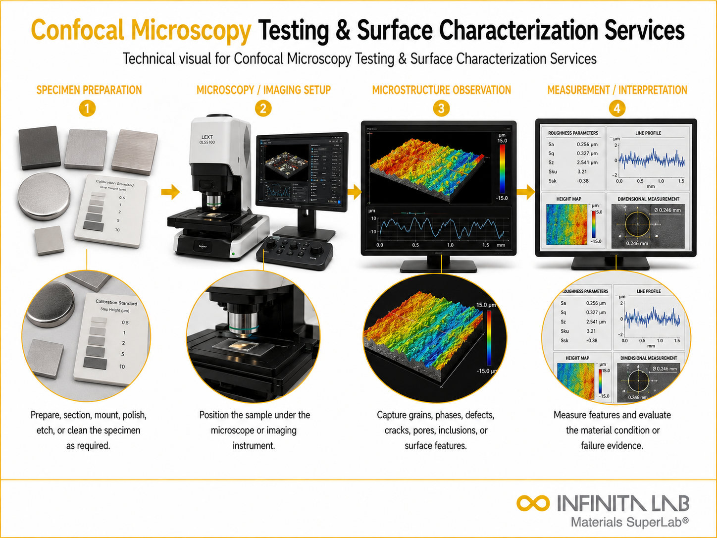
Test Process
Sample Preparation & Placement
The sample is cleaned to remove dust, oil, and contaminants, then placed and aligned on the microscope stage.
1Laser Scanning & Optical Sectioning
A focused laser scans the surface, and a pinhole blocks out-of-focus light to capture sharp images.
2Image Acquisition & 3D Reconstruction
Reflected or fluorescent signals are collected and combined to generate high-resolution 3D images.
3Data Analysis & Reporting
Surface parameters such as roughness, size, and thickness are measured and analyzed.
4Technical Specifications
| Parameter | Details |
|---|---|
| Applicable Materials | Polymers, metals, coatings, semiconductors, ceramics |
| Measurement Capability | Surface roughness, thickness, 3D profiling |
| Resolution | Sub-micron lateral resolution, nanometre-scale vertical resolution |
| Output Format | 2D images, 3D surface maps |


Instrumentation Used for Testing
- Confocal laser scanning microscope (CLSM)
- Laser source (visible or near-infrared)
- Objective lenses (high numerical aperture)
- Photodetector (PMT or CCD)
- Motorised stage
- Computer with image processing software
- 3D reconstruction software
Results and Deliverables
- High-resolution 2D images
- 3D surface topography maps
- Surface roughness values
- Layer thickness measurements
- Defect and feature analysis
- Comparative imaging reports
- Research and analysis reports
Frequently Asked Questions
Unlike conventional optical microscopy, confocal microscopy eliminates out-of-focus light using a pinhole, resulting in sharper images and the ability to capture depth (3D) information.
No, it is a non-destructive technique that does not damage the sample, making it suitable for delicate and high-value materials.
It can analyse solids such as metals, polymers, coatings, ceramics, semiconductors, and even soft or biological materials.
It provides surface roughness, layer thickness, microstructural details, 2D images, and 3D surface maps.
Minimal preparation is required. Typically, the sample needs to be clean and free from dust or contaminants.
Why Choose Infinita Lab for Advanced Materials Testing and Characterization?
At the core of this breadth is our network of 2,000+ accredited laboratories across the USA, offering access to over 10,000 testing methods and analytical services. From advanced materials characterization (SEM, TEM, RBS, XPS) to mechanical, chemical, environmental, biological, and standardized ASTM/ISO-compliant testing, we deliver unmatched flexibility, specialization, and scale. You are never limited by geography, facility, or methodology — Infinita Lab connects you to the right expertise and testing solution, every time.

Looking for a Trusted Partner for Accurate and Reliable Testing Services?
Send query us at hello@infinitlab.com or call us at (888) 878-3090 to learn more about our services and how we can support you.


Request a Quote
Submit your material details and receive testing procedures, pricing, and turnaround time within 24 hours.
 Quick Turnaround and Hasslefree process
 Confidentiality Guarantee
 Free, No-obligation Consultation
 100% Customer Satisfaction
