


Spectral Ellipsometry Testing Services
Spectral Ellipsometry is an optical technique that uses light to measure the composition and properties of thin films. Spectral ellipsometry can determine composition, roughness, crystalline nature, thickness, electrical conductivity, and other material properties.
TRUSTED BY


Get compliant results — request your spectral ellipsometry testing quote
- Overview
- Scope, Applications, and Benefits
- Test Process
- Specifications
- Instrumentation
- Results and Deliverables
What Is Spectral Ellipsometry?
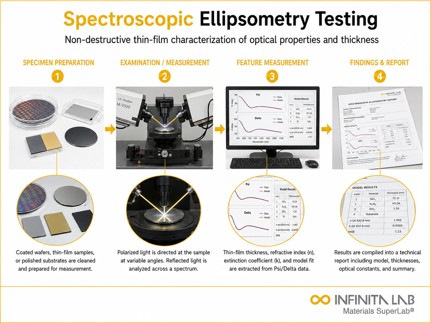
Spectroscopic ellipsometry (SE) is a non-destructive optical technique used to characterize thin films and surfaces by measuring the change in polarization state of light reflected from a sample. As polarized light strikes a film-coated surface, the amplitude ratio and phase difference between the p- and s-polarized reflected components (expressed as the ellipsometric parameters Ψ and Δ) are recorded across a range of wavelengths. By fitting these measured spectra to an optical model of the sample structure, spectroscopic ellipsometry determines film thickness, refractive index (n), and extinction coefficient (k) with sub-nanometer to nanometer precision.
Because the technique is sensitive to extremely thin layers and does not require sample destruction, spectroscopic ellipsometry is widely used in semiconductor, optics, coatings, and thin-film research to characterize single and multilayer film stacks, including films only a few atomic layers thick.

Applications and Benefits of Spectral Ellipsometry Testing
Scope
Spectroscopic ellipsometry applies to thin films and coated surfaces on reflective or semi-reflective substrates, including:
- Semiconductor thin films – oxide, nitride, polysilicon, and metal films on silicon and compound semiconductor wafers
- Optical coatings – anti-reflective, dielectric mirror, and filter coatings on glass or polymer substrates
- Polymer and organic films – spin-coated resists, organic electronic layers, and protective coatings
- Multilayer stacks – sequential layer structures where individual layer thickness and optical constants must be resolved
Applications
- Semiconductor process control – monitoring gate oxide, nitride, and polysilicon film thickness during wafer fabrication
- Optical coating development and verification – confirming layer thickness and refractive index of anti-reflective and multilayer optical coatings
- Material characterization – determining the optical constants (n, k) of new or unknown thin-film materials across the UV-visible-near-IR spectrum
- Surface roughness and interface analysis – assessing surface and interfacial roughness contributions to the measured optical response
- Failure analysis and reverse engineering – characterizing film stacks on failed or competitor devices to understand layer composition and thickness
Benefits
- Nanometer to sub-nanometer precision – ellipsometry resolves film thickness changes far below the wavelength of light used
- Non-destructive and non-contact – measurements are performed without damaging or altering the sample
- Simultaneous thickness and optical constant determination – a single measurement yields both physical thickness and the wavelength-dependent refractive index and extinction coefficient
- Sensitive to ultra-thin films – capable of characterizing films down to monolayer thickness, beyond the practical limit of many other thickness measurement techniques
- Applicable to complex multilayer structures – appropriate optical modeling allows individual layer properties to be extracted from stacks of several films
Spectroscopic Ellipsometry Testing Process
Sample Mounting
Position and align the sample on the ellipsometer stage.
1Measurement Setup
Select the required incidence angle and wavelength range.
2Data Acquisition and Modelling
Measure Ψ and Δ, then build an optical model of the film layers.
3Fitting and Reporting
Fit the model to determine film thickness, refractive index, extinction coefficient, and goodness of fit.
4Spectroscopic Ellipsometry Testing Technical Specifications
| Parameter | Details |
|---|---|
| Applicable Materials | Semiconductor films, optical coatings, polymer/organic films, multilayer stacks |
| Measured Parameters | Ellipsometric angles Ψ (amplitude ratio) and Δ (phase difference) |
| Derived Parameters | Film thickness, refractive index (n), extinction coefficient (k), surface/interface roughness |
| Typical Wavelength Range | Ultraviolet through near-infrared (approximately 190 nm to 2500 nm, instrument dependent) |
| Thickness Sensitivity | Sub-nanometer to nanometer resolution |
| Angle of Incidence | Typically variable, commonly 45°–75° from normal |
| Related Techniques | Reflectometry, profilometry, X-ray reflectivity (XRR) for complementary thickness verification |


- Spectroscopic ellipsometer with rotating analyzer, rotating compensator, or phase-modulated configuration
- Broadband light source spanning the UV, visible, and near-infrared spectral regions
- Polarizer, compensator, and analyzer optical components for polarization state control and detection
- Motorized sample stage with adjustable angle of incidence
- Optical modeling and data-fitting software with material dispersion libraries
Equipment and Instrumentation Used for Testing
What You Receive: Test Report, Data, and Certification
- Test report – documentation of sample identification, measurement configuration, and optical model used for data fitting
- Film thickness data – fitted thickness for each layer in the measured film stack
- Optical constants (n, k) – wavelength-dependent refractive index and extinction coefficient for each characterized layer
- Goodness-of-fit statistics – mean squared error or equivalent metric indicating the quality of the model fit to measured data
- Comparative analysis – side-by-side comparison of film properties across multiple samples, process conditions, or wafer locations
Spectral Ellipsometry FAQs
Polarised light is directed onto the specimen at a controlled angle, and the reflected light is measured. Changes in amplitude and phase are analysed using an optical model.
Testing can be performed on semiconductors, coatings, polymers, oxides, metals, solar-cell materials and optical films. It is especially useful for very thin layers deposited on reflective substrates.
No. The method is generally non-contact and non-destructive, allowing the specimen to remain unchanged after testing. It is suitable for research, process development and production quality control.
An optical model represents the substrate, individual layers, roughness and material properties of the specimen. Measured data are fitted to the model to calculate thickness and optical constants.
It is widely used in semiconductor manufacturing, photovoltaics, display technology, optical coatings and nanomaterials research. It supports deposition-process control and thin-film characterisation.
Why Choose Infinita Lab for Spectral Ellipsometry Testing
At the core of this breadth is our network of 2,000+ accredited laboratories across the USA, offering access to over 10,000 testing methods and analytical services. From advanced materials characterization (SEM, TEM, RBS, XPS) to mechanical, chemical, environmental, biological, and standardized ASTM/ISO-compliant testing, we deliver unmatched flexibility, specialization, and scale. You are never limited by geography, facility, or methodology — Infinita Lab connects you to the right expertise and testing solution, every time.

Looking for an Accredited Partner for Spectral Ellipsometry Testing?
Send query us at hello@infinitalab.com or call us at (888) 878-3090 to learn more about our services and how we can support you.



Request a Quote
Submit your material details and receive testing procedures, pricing, and turnaround time within 24 hours.
 Quick Turnaround and Hasslefree process
 Confidentiality Guarantee
 Free, No-obligation Consultation
 100% Customer Satisfaction
