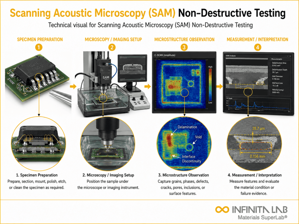


What Is Scanning Acoustic Microscopy SAM?
The process of Scanning Acoustic Microscopy (SAM) analysis is non-destructive and can be employed to detect and evaluate internal defects, delaminations, voids, cracks, and disbonds within electronic, semiconductor, and materials assemblies without sectioning or destroying the specimen. High-resolution internal defect mapping and material integrity data are obtained using SAM, providing critical non-destructive inspection information for failure analysis, quality engineers, and materials researchers.
Applications and Benefits of Scanning Acoustic Microscopy SAM Testing
Scope
A focused ultrasonic beam is directed into the specimen by SAM, and reflected acoustic signals are collected from within interfaces, defects, and material discontinuities, creating detailed acoustic images that show structural integrity, delamination, voids, and interface conditions in specific inspection planes without damaging the specimen.
SAM analysis evaluates:
- Internal delamination, void, and crack detection within electronic packages and semiconductor devices
- Die attach, underfill, and encapsulant integrity assessment in assembled electronic components
- Interface disbond and adhesion failure identification across dissimilar material boundaries
- Moisture-induced delamination and popcorning damage in plastic-encapsulated devices
- Internal structural integrity of advanced composite, ceramic, and bonded material assemblies
Applications
- Semiconductor packages, BGAs, flip-chip, and CSP devices requiring internal defect inspection
- Electronic assemblies and PCB components requiring non-destructive internal integrity assessment
- Automotive, aerospace, and defense electronic modules
- Adhesively bonded, composite, and multilayer material assemblies requiring interface integrity evaluation
- Failure analysis investigations requiring non-destructive internal defect characterization before sectioning
Benefits
- Provides non-destructive internal defect detection without specimen sectioning or destruction
- Identifies delamination, voids, and interface disbonds invisible to conventional optical inspection
- Delivers traceable, laboratory-certified acoustic inspection data for failure analysis
- Reduces failure analysis time by non-destructively mapping internal defects before destructive sectioning
Our Testing Procedure
Sample Preparation
Specimens are cleaned, dimensioned, and immersed in the acoustic coupling medium within the SAM analysis system, with scan parameters configured for the target inspection depth and resolution requirements.
1Acoustic Scanning
A focused ultrasonic transducer scans across the specimen surface, transmitting acoustic pulses into the material and collecting reflected signals from internal interfaces, defects, and material discontinuities.
2Acoustic Image Generation
Reflected acoustic signal amplitude and time-of-flight data are processed to generate high-resolution C-scan, B-scan, and A-scan acoustic images revealing internal defect distribution and material integrity.
3Defect Analysis & Reporting
Acoustic images are analyzed for defect identification, classification, and sizing to determine test compliance result.
4Test parameters and requirements
| Parameter | Details |
|---|---|
| Applicable Materials | Semiconductor packages, electronic assemblies, adhesive bonds, composites, and multilayer systems |
| Inspection Technique | Focused ultrasonic pulse-echo and through-transmission scanning with C-scan, B-scan, and A-scan imaging |
| Spatial Resolution | High-resolution internal defect detection dependent on transducer frequency and material properties |
| Measured Parameters | Internal delamination, void distribution, crack extent, and interface disbond |
| Measured Outputs | C-scan images, B-scan cross-sections, defect maps, sizing data, and test compliance result |


- Calibrated scanning acoustic microscopy system with focused ultrasonic transducer array
- High-frequency ultrasonic pulse generation and signal acquisition electronics
- Acoustic coupling medium tank with temperature-controlled immersion system
- Precision XY scanning stage for high-resolution specimen raster scanning
- Specialist acoustic image acquisition, processing, and defect analysis software
- Data reporting and image visualization system
Equipment and Instrumentation Used for Testing
What You Receive: Test Report, Data, and Certification
- High-resolution C-scan acoustic images revealing internal defect distribution across inspection planes
- B-scan cross-sectional acoustic images for defect depth and extent characterization
- Defect identification, classification, and sizing data for all detected internal anomalies
- Test compliance result assessed against defined internal inspection acceptance criteria
- SAM analytical report
Scanning Acoustic Microscopy SAM FAQs
Scanning Acoustic Microscopy is a non-destructive inspection technique that uses ultrasonic waves to detect and display internal delaminations, voids, cracks, and interfacial disbonds within electronic packages, semiconductor devices, and material systems, without requiring specimen sectioning or destructive preparation.
SAM is used for internal delaminations, voids, cracks, interfacial disbonds, die-attach failures, underfill delaminations, moisture-induced popcorn damage, and adhesion failures. These internal structural defects in electronic devices and materials cannot be detected by conventional optical or visual inspection.
Inspection of semiconductor packages, BGAs, flip chip packages, CSPs, electronic components in PCBs, adhesively bonded structures, composite structures, ceramic components, and multilayer material systems is all possible with SAM. Internal integrity information is provided in a non-destructive fashion.
SAM is used to non-destructively examine internal defects, delaminations, and interfacial anomalies within electronic packages and material structures prior to destructive cross-sectioning, allowing failure analysts to identify and locate internal defect sites for cross-section analysis.
This SAM analysis is utilized in various industries, including semiconductor, electronics, automotive, aerospace, and advanced materials, for electronic package qualification, incoming inspection, failure analysis, adhesive bond integrity, and internal defect characterization, which require non-destructive inspection capability.
Scanning Acoustic Microscopy (SAM) failure analysis is a nondestructive technique used to identify internal defects and investigate failure mechanisms in semiconductor packages, electronic components, and multilayer materials. The technique uses high-frequency ultrasonic waves transmitted through a water coupling medium into the specimen. When the waves encounter interfaces between different materials or defects, such as air gaps, cracks, or delamination, part of the signal is reflected back to the transducer. The reflected signals are processed to generate detailed images of the specimen's internal structure. These images help identify defects such as voids, delamination, cracks, and bonding failures, supporting root-cause analysis and product reliability assessment.
Why Choose Infinita Lab for Scanning Acoustic Microscopy SAM Testing?
When your Scanning Acoustic Microscopy SAM results have to hold up - for compliance, a customer audit, or an engineering decision - accuracy and an unbiased third-party report matter more than price. Infinita Lab routes your scanning acoustic microscopy SAM testing to ISO/IEC 17025-accredited U.S. partner labs with hands-on method experience, so you get defensible data, transparent reporting, and turnaround times built around your project deadline - not ours.

Looking for an Accredited Partner for Scanning Acoustic Microscopy SAM Testing?
Send query us at hello@infinitalab.com or call us at (888) 878-3090 to learn more about our services and how we can support you.