


PCB Analysis Testing Services
Printed Circuit Board (PCB) analysis includes the following; measuring various plate thicknesses, identifying foreign materials, discovering defective parts, and also using cross-sectional examinations. Printed Circuit Boards (PCBs), also referred to as Printed Wiring Boards (PWBs) or Etched Wiring Boards (EWBs), are electronic circuits used in devices to provide mechanical support and a source of way to their electronic parts.
TRUSTED BY


Get compliant results — request your PCB analysis testing quote
- Overview
- Scope, Applications, and Benefits
- Test Process
- Specifications
- Instrumentation
- Results and Deliverables
What Is PCB Analysis?
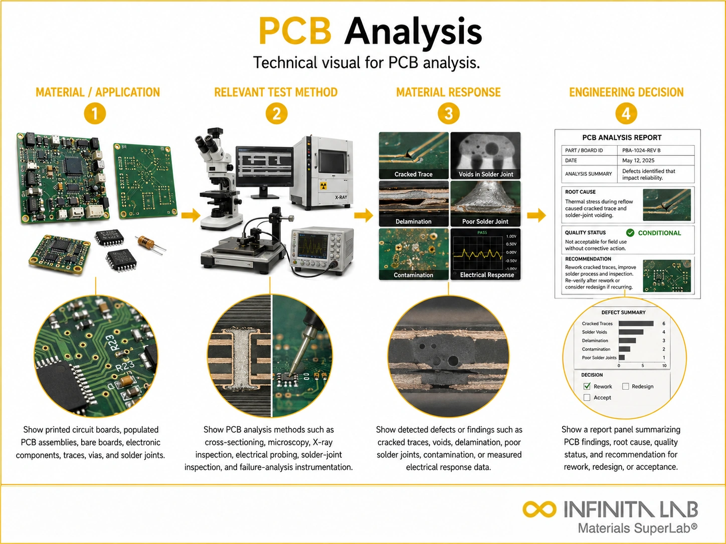
Printed circuit board (PCB) analysis encompasses the full range of physical, chemical, and structural examinations performed on bare boards, assembled boards, and individual components to understand how they were made, how they perform, and why they failed. PCBs are complex multilayer structures -copper traces, laminate substrates, plated through-holes, surface finishes, solder joints, and embedded components all packed into a stack that may be less than two millimeters thick. When something goes wrong, getting to the root cause requires tools and techniques that can see and characterize features at the micron level.
The most widely used approach for PCB structural analysis is cross-sectioning, where a board is mounted in epoxy, sectioned, polished, and examined under optical or electron microscopy. This reveals plating thickness, hole wall quality, laminate integrity, solder joint microstructure, via fill, and layer-to-layer registration -all of which directly affect board reliability. Non-destructive methods, including X-ray inspection and scanning acoustic microscopy (SAM), are used first when the board needs to be preserved or when internal defects need to be located before destructive analysis begins.
Chemical and elemental analysis adds another dimension -identifying surface contamination, verifying surface-finish composition, analyzing solder alloys, detecting ionic residues that can cause corrosion or leakage, and confirming that materials meet RoHS and halogen-free requirements. At Infinita Lab, we connect clients with labs equipped for the full spectrum of PCB analysis, from routine cross-section inspection to advanced failure analysis involving FIB, TEM, and trace-contamination identification.

Applications and Benefits of PCB Analysis Testing
Scope
PCB analysis covers bare boards, populated assemblies, and individual components across all board constructions, including single-sided, double-sided, multilayer, rigid, flexible, and rigid-flex. Analysis types include structural and dimensional characterization via cross-sectioning, optical microscopy, and SEM; non-destructive internal inspection via X-ray and scanning acoustic microscopy; surface and elemental analysis by SEM-EDS, XRF, and FTIR; ionic contamination testing; solder joint and intermetallic characterization; and failure analysis investigations for opens, shorts, delamination, cratering, pad lifting, and other defect modes. Relevant industry standards include IPC-A-600, IPC-6012, IPC-TM-650, J-STD-001, and IPC-7711/7721 for artistry and acceptance criteria, as well as IEC 62321 for material content testing.
Applications
- Cross-section analysis for plating thickness, hole wall quality, and layer registration verification
- Solder joint inspection and intermetallic compound (IMC) layer characterization
- Failure analysis for field returns, delamination, opens, shorts, and pad cratering.
- Surface finish verification -ENIG, HASL, OSP, immersion silver, ENEPIG
- Ionic contamination and cleanliness testing per IPC-TM-650 2.3.25 and J-STD-001
- RoHS material content screening and solder alloy verification by XRF
- Halogen-free material verification for FR4 laminate and solder mask
- Incoming board inspection and supplier quality audit support
- New design qualification and process validation for PCB fabricators and assemblers
- Counterfeit component detection and authentication
Benefits
- Cross-sectioning reveals an internal board structure that no surface inspection can access.
- Non-destructive X-ray and SAM allow defect location before committing to destructive analysis.
- Combines structural, elemental, and chemical analysis under one coordinated investigation
- Covers the full supply chain -from raw laminate to assembled and soldered boards
- Findings referenced against IPC acceptance criteria provide context beyond raw measurements.
- Identifies failure mechanisms that guide corrective action rather than just confirming a failure exists
- Applicable to consumer electronics, aerospace, medical devices, automotive, and industrial boards
PCB Analysis & Inspection Testing Process
Non-Destructive Inspection
X-ray imaging is used to inspect internal features, including via fill, solder joint voids
1Cross-Sectioning and Structural Analysis
The board is mounted in epoxy, sectioned at the region of interest, and progressively ground and polished to expose the target feature plane.
2Surface and Chemical Analysis
Surface finish composition, solder alloy identity, and elemental composition of deposits or corrosion products are characterized by XRF or SEM-EDS.
3Root Cause Assessment and Reporting
All findings are compiled and correlated to develop a root cause assessment.
4Test parameters and requirements
| Parameter | Details |
|---|---|
| Service Type | Multi-technique analytical service -the analysis objective drives method selection |
| Board Types | Bare boards, assembled boards, rigid, flexible, rigid-flex, single to high-layer-count multilayer |
| Non-Destructive Methods | X-ray inspection (2D and CT), scanning acoustic microscopy (SAM) |
| Structural Analysis | Cross-sectioning, optical microscopy, SEM |
| Elemental and Surface Analysis | SEM-EDS, XRF, FTIR, Raman spectroscopy |
| Contamination Testing | ROSE test, ion chromatography (IPC-TM-650 2.3.25), ionic contamination mapping |
| Relevant Standards | IPC-A-600, IPC-6012, IPC-TM-650, J-STD-001, IEC 62321 |


- X-ray inspection system (2D radiography and computed tomography)
- Scanning acoustic microscope (SAM)
- Precision sectioning saw, mounting press, and polishing system
- Optical microscope with measurement software
- Scanning electron microscope (SEM) with energy dispersive X-ray spectroscopy (EDS)
- X-ray fluorescence (XRF) spectrometer for surface finish and alloy verification
- FTIR spectrometer and microscope for organic contamination and residue identification
- Ion chromatography system for ionic contamination quantification
- ROSE tester for bulk ionic cleanliness measurement
Equipment and Instrumentation Used for Testing
PCB Analysis & Inspection Results and Deliverables
- Cross-section images with measurements -plating thickness, hole wall integrity, layer registration
- Solder joint microstructure images and intermetallic compound (IMC) thickness data
- X-ray and SAM images showing internal voids, delamination, or component placement issues
- Elemental composition data for surface finishes, solder alloys, and deposits
- Ionic contamination levels in comparison to IPC cleanliness limits
- Material content screening results for RoHS-restricted substances
- Defect identification with probable mechanism and origin assessment for failure analysis cases
- Full analytical report with all images, data, measurements, and conclusions formatted for engineering and quality review
PCB Analysis FAQs
PCB analysis can identify issues such as trace cracking, delamination, via failures, solder joint defects, corrosion, conductive anodic filament (CAF) growth, and thermal or electrical damage.
Yes. By examining the PCB's physical condition and failure characteristics, engineers can often distinguish between manufacturing defects, assembly-related issues, and failures caused by operational or environmental stresses.
Depending on the failure mode, techniques may include X-ray inspection, cross-sectioning, optical microscopy, SEM/EDS analysis, scanning acoustic microscopy, and electrical continuity testing.
Yes. Non-destructive methods such as X-ray imaging and scanning acoustic microscopy are often used first to locate internal defects before any destructive analysis is considered.
Providing the PCB design details, failure symptoms, operating conditions, assembly history, test results, and known-good comparison samples helps improve the accuracy and efficiency of the root cause investigation.
Why Choose Infinita Lab for PCB Analysis Testing
At the core of this breadth is our network of 2,000+ accredited laboratories across the USA, offering access to over 10,000 testing methods and analytical services. From advanced materials characterization (SEM, TEM, RBS, XPS) to mechanical, chemical, environmental, biological, and standardized ASTM/ISO-compliant testing, we deliver unmatched flexibility, specialization, and scale. You are never limited by geography, facility, or methodology — Infinita Lab connects you to the right expertise and testing solution, every time.

Looking for an Accredited Partner for PCB Analysis Testing?
Send query us at hello@infinitalab.com or call us at (888) 878-3090 to learn more about our services and how we can support you.



Request a Quote
Submit your material details and receive testing procedures, pricing, and turnaround time within 24 hours.
 Quick Turnaround and Hasslefree process
 Confidentiality Guarantee
 Free, No-obligation Consultation
 100% Customer Satisfaction
