

What Is Atom Probe Tomography?
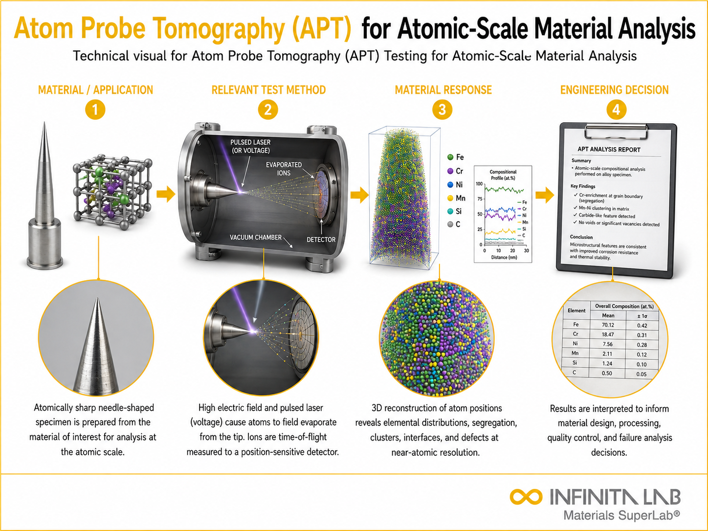
Atom Probe Tomography is a highly advanced microscopy and analysis technique used to identify the 3D atomic structure of materials. It is a technique whereby a strong electric field is applied to a needle-shaped sample of material, causing atoms to evaporate from its surface.
APT is a highly advanced microscopy and analysis technique with very high resolution, allowing scientists to identify the location of atoms within a given material. It is commonly used to study materials at the atomic level across various fields, including materials science, nanotechnology, metallurgy, semiconductors, and advanced alloys.

Applications and Benefits of Atom Probe Tomography Testing
Scope
Atom Probe Tomography is used to analyze the atomic composition and spatial distribution of elements within materials at near-atomic resolution. The technique enables detailed investigation of nanoscale structures and interfaces.
The scope includes:
Atomic-scale elemental composition analysis
Three-dimensional atomic structure mapping
Analysis of nanomaterials and alloys
Characterization of thin films and interfaces
Detection of trace elements and impurities
Applications
Semiconductor and microelectronics research
Metallurgy and alloy development
Nanomaterials characterization
Thin film and interface analysis
Materials failure and defect investigation
Benefits
Provides near-atomic resolution imaging
Enables 3D reconstruction of atomic structures
Detects very small concentrations of elements
Helps study nanoscale material behavior
Supports advanced materials research and development
Our Testing Procedure
Sample Preparation
The material is prepared into a very sharp needle-shaped specimen, often using focused ion beam techniques.
1Field Evaporation
A strong electric field combined with laser or voltage pulses causes atoms to evaporate from the sample surface.
2Ion Detection
The evaporated ions travel to a position-sensitive detector that records their identity and location.
33D Reconstruction
The detected data is processed to reconstruct a three-dimensional atomic map of the material.
4Test parameters and requirements
| Parameter | Details |
|---|---|
| Spatial Resolution | Sub-nanometer to atomic scale |
| Detection Method | Time-of-flight mass spectrometry |
| Sample Shape | Needle-shaped specimen (~50–100 nm tip radius) |
| Operating Environment | Ultra-high vacuum |
| Ion Source | Field evaporation using voltage or laser pulses |
| Analysis Capability | Elemental identification and 3D mapping |
| Output Data | Atomic position and composition maps |


Atom Probe Tomography System
Laser or Voltage Pulse Generator
Position-Sensitive Ion Detector
Ultra-High Vacuum Chamber
Data Reconstruction and Analysis Software
Equipment and Instrumentation Used for Testing
What You Receive: Test Report, Data, and Certification
3D atomic structure reconstruction
Elemental composition mapping
Detection of impurities and nano-segregation
Interface and phase analysis
Detailed atomic-scale characterization report
Atom Probe Tomography FAQs
Atom Probe Tomography is an advanced microscopy technique that identifies and maps individual atoms in a material, allowing researchers to study its three-dimensional atomic structure and elemental composition.
APT provides near-atomic spatial resolution and precise chemical identification, allowing researchers to visualize the exact position of atoms and analyze nanoscale material structures.
APT can detect features at the atomic scale, often below one nanometer, making it one of the most precise techniques for nanoscale material analysis.
Ultra-high vacuum conditions prevent contamination and ensure accurate detection of ions evaporated from the specimen during analysis.
APT allows scientists to study atomic-scale structures, detect trace elements, and understand nanoscale material behavior, which is essential for developing advanced materials and improving product performance.
Atom probe tomography (APT) is an advanced materials characterization technique that identifies individual atoms and maps their three-dimensional distribution. A sample is prepared as a sharp needle-shaped tip and cooled under controlled conditions. A high electric field, combined with voltage or laser pulses, removes atoms as ions from the tip. A detector records their arrival times and impact positions, allowing software to reconstruct the material’s atomic-scale composition and structure.
Atom probe analysis determines the chemical composition and spatial distribution of atoms within a small region of a material. A needle-shaped specimen is exposed to a high electric field, causing atoms to evaporate as ions. Their time of flight is measured to determine their mass-to-charge ratios, while detector positions help establish their original locations. The resulting data reveal elemental distributions, impurities, and nanoscale segregation.
Atom probe tomography works by sequentially removing atoms from a sharp specimen and detecting them individually. The instrument combines field evaporation with time-of-flight mass spectrometry to identify the ions and a position-sensitive detector to record where they arrive. These measurements are used to generate a three-dimensional atomic map, helping researchers investigate alloy composition, grain boundaries, interfaces, and nanoscale precipitates.
Why Choose Infinita Lab for Atom Probe Tomography Testing
When your Atom Probe Tomography results have to hold up - for compliance, a customer audit, or an engineering decision - accuracy and an unbiased third-party report matter more than price. Infinita Lab routes your atom probe tomography testing to ISO/IEC 17025-accredited U.S. partner labs with hands-on method experience, so you get defensible data, transparent reporting, and turnaround times built around your project deadline - not ours.

Looking for an Accredited Partner for Atom Probe Tomography Testing?
Send query us at hello@infinitalab.com or call us at (888) 878-3090 to learn more about our services and how we can support you.