


Semiconductor
Verification of semiconductors guarantees that the components in today’s devices operate reliably, uniformly, and with high efficiency. Infinita Lab provides complete test solutions, including electrical characterization, heat testing, dielectric power testing, environmental testing, and surface analysis. Tests of this kind guarantee device functioning in diverse circumstances and define defectiveness in the early stages of production. Through the assessment of primary parameters such as conductivity, carrier lifetime, and electrostatic protection, we assist manufacturers in boosting device reliability, averting failures, and aligning with global standards—enabling innovation and performance in the fast-transforming semiconductor sector.
Top Semiconductor Testing Services
-
 Plasma Focused Ion Beam (P-FIB): How It Works & Applications
 -
What Is SIMS (Secondary Ion Mass Spectrometry)? Principle & Applications
-
ToF-SIMS: Principles, Techniques & Applications Guide
-
 What Is Electron Energy Loss Spectroscopy (EELS)? Principles & Applications
 -
Characterization Techniques for Thin Film Organic Coatings: Methods & Metrology
-
4D-STEM Testing for Nanoscale Strain & Electric Field Mapping


Industries We Serve


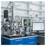
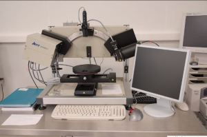
Semiconductor Testing Services
Semiconductors constitute the fundamental architecture of modern electronic systems, including mobile telecommunications devices and electric vehicles. These essential components facilitate the sophisticated operation of microprocessors, sensors, power management devices, and integrated circuits. To ensure optimal performance and the absence of defects during both fabrication and operational deployment, rigorous, standardized testing protocols are mandatory.
Infinita Lab delivers a comprehensive suite of analytical solutions, encompassing electrical characterization, thermal evaluation, dielectric power assessment, environmental stress testing, and detailed surface analysis. These specialized services validate device functionality under diverse environmental conditions and facilitate proactive identification of manufacturing anomalies. By systematically evaluating critical parameters such as electrical conductivity, carrier lifetime, and electrostatic discharge protection, Infinita Lab assists manufacturers in augmenting device reliability, mitigating potential failure modes, and ensuring strict adherence to international regulatory standards.
Infinita Lab provides technical support to engineering teams and manufacturing entities by maintaining rigorous alignment with global quality and compliance frameworks, including internationally recognized standards such as ASTM and ISO 17025.
Semiconductor Testing Services Offered by Infinita Lab
Electrical Characterization- Resistivity & Hall Effect Testing
Comprehending the flow of electric charge through semiconductor materials is fundamental to device testing. Resistivity and Hall-effect measurements provide precise insights into carrier-level behavior during wafer qualification, batch verification, and fabrication process monitoring.
ASTM F76 specifies test methods for determining the electrical properties of single-crystal semiconductors, including resistivity, Hall coefficient, and Hall mobility. The test evaluates how charge carriers behave within the material under the influence of an applied electric current and magnetic field. This method is widely used for semiconductor materials, such as silicon and compound semiconductors, to assess the type of conductivity, carrier concentration, and mobility. The results are critical for material characterization, process control, and performance evaluation in electronic device manufacturing.
Key parameters measured include electrical resistivity, Hall coefficient, carrier concentration, Hall mobility, and conductivity type (n-type or p-type).
Electrical Conductivity Testing- Eddy Current Method
Eddy current testing is a rapid, non-destructive method for assessing the electrical conductivity of metallic interconnects, lead frames, heat spreaders, and packaging materials. This contactless technique facilitates real-time alloy identification and heat-treatment verification.
Relevant ASTM Standards:
ASTM E1004: Standard test method using the electromagnetic (eddy-current) technique to measure the electrical conductivity of nonmagnetic metals. The technique is based on measuring the eddy currents induced in the material and analyzing the results to infer its conductivity. When used with reference standards of known values, ASTM E1004 provides accurate and repeatable results. The technique applies to metals with flat or slightly curved surfaces, even when they have thin non-conductive coatings.
ASTM E1004 evaluates the effects of conductivity type, heat treatment, alloy aging, corrosion, and heat damage. These capabilities make it valuable for incoming inspection, production monitoring, and failure analysis.
Surface & Volume Resistivity Testing
Controlling static electricity in semiconductor manufacturing is essential, as undetected electrostatic discharge can cause irreversible device damage. Resistivity testing of packaging, trays, work surfaces, and enclosures protects sensitive components from ESD damage.
Relevant ASTM Standards:
ASTM D257– The primary standard for measuring DC surface and volume resistivity of electrical insulating materials. It specifies the use of a guarded electrode system- a three-terminal electrode configuration that separates the measured volume current from surface leakage currents. In the electronics industry, uncontrolled static discharge (ESD) can destroy sensitive semiconductor components at energy levels invisible to the human senses. Antistatic and ESD-dissipative materials with controlled resistivity are used in packaging, flooring, work surfaces, and garments throughout electronics manufacturing environments.
Dielectric Strength Testing
Each insulating layer in a semiconductor device must withstand voltage stress. Dielectric breakdown can result in device malfunction or failure. Testing breakdown voltage before market release is a critical quality assurance measure.
Relevant ASTM Standards:
ASTM D149– Standard test method for dielectric breakdown voltage and dielectric strength of solid electrical insulating materials, measuring the highest voltage a material can sustain before electrical failure. This test is essential for qualifying semiconductor packaging materials, gate insulators, and dielectric films used in power devices and integrated circuits.
Dielectric Constant & Dissipation Factor Testing
As semiconductor devices operate at higher speeds and frequencies, the dielectric properties of surrounding materials become increasingly important. Substrates or encapsulants with elevated dielectric constants can impede signal transmission and induce crosstalk. Accurate material characterization at operational frequencies supports optimal device design.
Relevant ASTM Standards:
ASTM D150– Standard test method for AC loss characteristics and permittivity (dielectric constant) of solid electrical insulation, measuring the dielectric constant and dissipation factor of materials used in semiconductor substrates, PCB laminates, and electronic encapsulants across a range of frequencies and temperatures.
ASTM D2520– Standard test methods for complex permittivity (dielectric constant) of solid electrical insulating materials at microwave frequencies and temperatures up to 1650°C, applicable to advanced semiconductor packaging ceramics and high-frequency substrate materials.
Thermal Characterization of Semiconductor Materials
Thermal management is essential for semiconductor performance. As device dimensions decrease and power densities increase, efficient heat dissipation becomes increasingly challenging. Thermal characterization of packaging, substrates, interface materials, and heat spreaders provides essential data for device stability and reliability.
Relevant ASTM Standards:
ASTM E1269– DSC determination of specific heat capacity of semiconductor packaging materials, thermal interface compounds, and substrate materials, providing essential thermophysical data for device thermal management design and simulation.
ASTM E1131 – Thermogravimetric Analysis (TGA) for compositional analysis, decomposition onset temperature, and thermal stability of semiconductor encapsulants, polymer packaging materials, and dielectric films – critical for qualifying materials in high-temperature processing environments.
ASTM E831– Coefficient of Linear Thermal Expansion (CTE) testing by TMA, quantifying the dimensional change of semiconductor packaging materials across temperature ranges- essential for managing thermal stress at solder joints, die attach interfaces, and substrate assemblies.
Dielectric Power & Breakdown Testing for Semiconductor Packaging
Power semiconductor devices, including IGBTs, MOSFETs, and SiC and GaN components, operate at voltages and switching speeds that impose significant stress on encapsulation and insulation systems. Verifying that packaging materials maintain dielectric integrity under operational conditions is essential for safety and reliability.
Relevant ASTM Standards:
ASTM D6097– Standard test method for relative resistance to vented water tree growth in solid dielectric insulating materials, evaluating the long-term insulation reliability of polymer materials used in cable insulation and semiconductor encapsulation systems exposed to electrical and moisture stress.
Environmental & Reliability Testing
A semiconductor device that performs well in laboratory settings must also withstand humidity, temperature fluctuations, and mechanical shock in operational environments. Environmental testing exposes devices to these conditions to verify reliability and durability.
Infinita Lab conducts rigorous environmental tests, including humidity resistance and temperature cycling. These simulations assess the ability of semiconductor devices to withstand mechanical and thermal stress during operation.
Relevant ASTM Standards:
ASTM E595 – Outgassing test for materials intended for use in space and vacuum environments, measuring total mass loss (TML) and collected volatile condensable materials (CVCM) from semiconductor packaging materials, adhesives, and encapsulants – critical for space-grade and high-reliability semiconductor applications.
Carrier Lifetime & Electrical Performance Testing
Carrier lifetime measurement determines the duration that charge carriers, such as holes and electrons, remain active in semiconductor materials. These data are essential for optimizing the efficiency and speed of components, including photovoltaic cells, transistors, and diodes.
Carrier lifetime directly influences leakage current, switching speed, and overall device efficiency. For example, short carrier lifetimes in silicon substrates can cause unexpected power losses in solar cells and bipolar transistors.
Why Semiconductor Testing Matters
Semiconductor testing is essential for ensuring the integrity, safety, and performance of modern electronic devices. As designs become more complex, even minor faults can result in numerous defective units. Rigorous testing ensures that products meet specifications, operate safely in diverse environments, and allow manufacturers to detect defects early, enhance reliability, reduce recall costs, and verify application compatibility.
Frequently Asked Questions
Semiconductor material testing is a crucial process that evaluates and analyzes the properties and characteristics of semiconductor materials used in electronic devices and integrated circuits. These materials, primarily silicon, but also compound semiconductors like gallium arsenide, are essential for modern electronics, serving as the foundation for transistors, diodes, and other electronic components. The process includes assessing the electrical, thermal, mechanical, and structural properties of these materials.
Environmental considerations are also considered in the semiconductor industry, with material testing assessing the environmental impact of materials, including energy efficiency and recyclability. Overall, Infinita Lab ensures semiconductor material testing is vital for ensuring the quality, reliability, and safety of electronic devices and integrated circuits.
Infinita Lab’s approach to semiconductor testing sets a superior standard in the U.S. due to its comprehensive and innovative methodologies. Leveraging state-of-the-art equipment and methodologies, our lab ensures unparalleled accuracy in assessing semiconductor performance. Unlike many other labs, Infinita Lab offers an extensive array of more than 2000 tests, ensuring a wide range of semiconductor properties are meticulously evaluated. Our team of experts is adept in the latest semiconductor technologies, offering not just testing services, but insightful consultations and customized solutions. This blend of technology, expertise, and customer-centric services ensures that clients receive not only results but also strategic insights, making Infinita Lab a leader in semiconductor testing.
At Infinita Lab, we excel in handling urgent semiconductor testing requirements and cater to projects with custom testing needs. Our agile and experienced team is equipped to respond swiftly to time-sensitive projects, ensuring a quick turnaround without compromising accuracy. Whether it’s a specialized testing request or an urgent project, we pride ourselves on our flexibility and commitment to meeting unique client needs. Trust Infinita Lab to deliver efficient and reliable semiconductor testing services tailored to your specific requirements, even under tight deadlines. Your urgency is our priority.
At Infinita Lab, streamlining end-to-end semiconductor testing services is achieved through a fusion of advanced technology and expert collaboration. Our approach begins with a comprehensive consultation to understand specific client needs, followed by the deployment of a suite of over 2000 specialized tests. Utilizing state-of-the-art equipment, we conduct thorough electrical, physical, and environmental analyses, ensuring precision at every step. Our expert team, proficient in the latest semiconductor technologies, provides insightful analysis and rapid turnaround times. We integrate seamless communication and data reporting, offering clients clear, actionable insights. This cohesive and efficient process exemplifies Infinita Lab’s commitment to delivering excellence in semiconductor testing services.
Read Our Blogs and Research Papers
In-depth examination of genuine material testing solutionsXenon Arc Exposure Testing: How It Works & Material Weathering Guide

Xenon Arc Exposure Testing: How It Works & Material Weathering Guide
Every material that is used outdoors — whether a vehicle coating, a roofing membrane, a textile canopy, or a plastic...
Read ArticleFiber Optics Testing: Methods, Standards & Material Performance Analysis
Fiber Optics Testing: Methods, Standards & Material Performance Analysis
What Is Fiber Optics Testing? Fiber-optic testing is the systematic evaluation of optical fiber cables, connectors, splices, and complete fiber-optic...
Read ArticleCommon Uses of Environmental Vibration Testing for Electrical Products
Common Uses of Environmental Vibration Testing for Electrical Products
Every product that moves — or exists in an environment that moves — is subject to vibration. Aircraft avionics experience...
Read Article
Get your Ceramic Material testing done from the largest network of accredited labs in the USA
We are a material testing lab with a vast network of accredited labs across the country. Our state-of-the-art equipment and experienced team provide accurate and timely testing services to meet the unique needs of our clients. Partner with us for reliable material testing solutions.
 Quick Turnaround and Hasslefree process
- Confidentiality Guarantee
- Free, No-obligation Consultation
- 100% Customer Satisfaction
